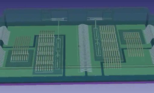
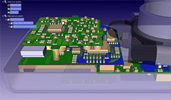
Concurrent design of multiple PCBs and Chip-Packages in a single environment
Design Force combines traditional 2D design with native 3D design and the latest human interface techniques, accelerated graphics, and almost instantaneous rendering and refreshing. Given these points, it is the fastest, most effective multi-board PCB design software available today. Design Force enables design teams to layout their designs in the context of a complete system or product.
Concurrent design of multiple PCBs and Chip-Packages in a single environment

Hierarchical multi-board PCB design and system-level signal and design traceability

Single environment for high-speed design with constraint management and SI and PI analysis

Design to any manufacturing specification with built-in design for manufacturing (DFM) checks
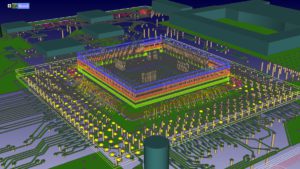
With a native 2D and 3D architecture, designers can effectively co-design a chip, package, and board to optimize I/Os at each level, embed components in the dielectric of a stack-up intelligently, and verify manufacturing rules in real-time.
Concurrent design-for-manufacturing checks and constraint verification ensure that both manufacturing and engineering intent are maintained during the design process.
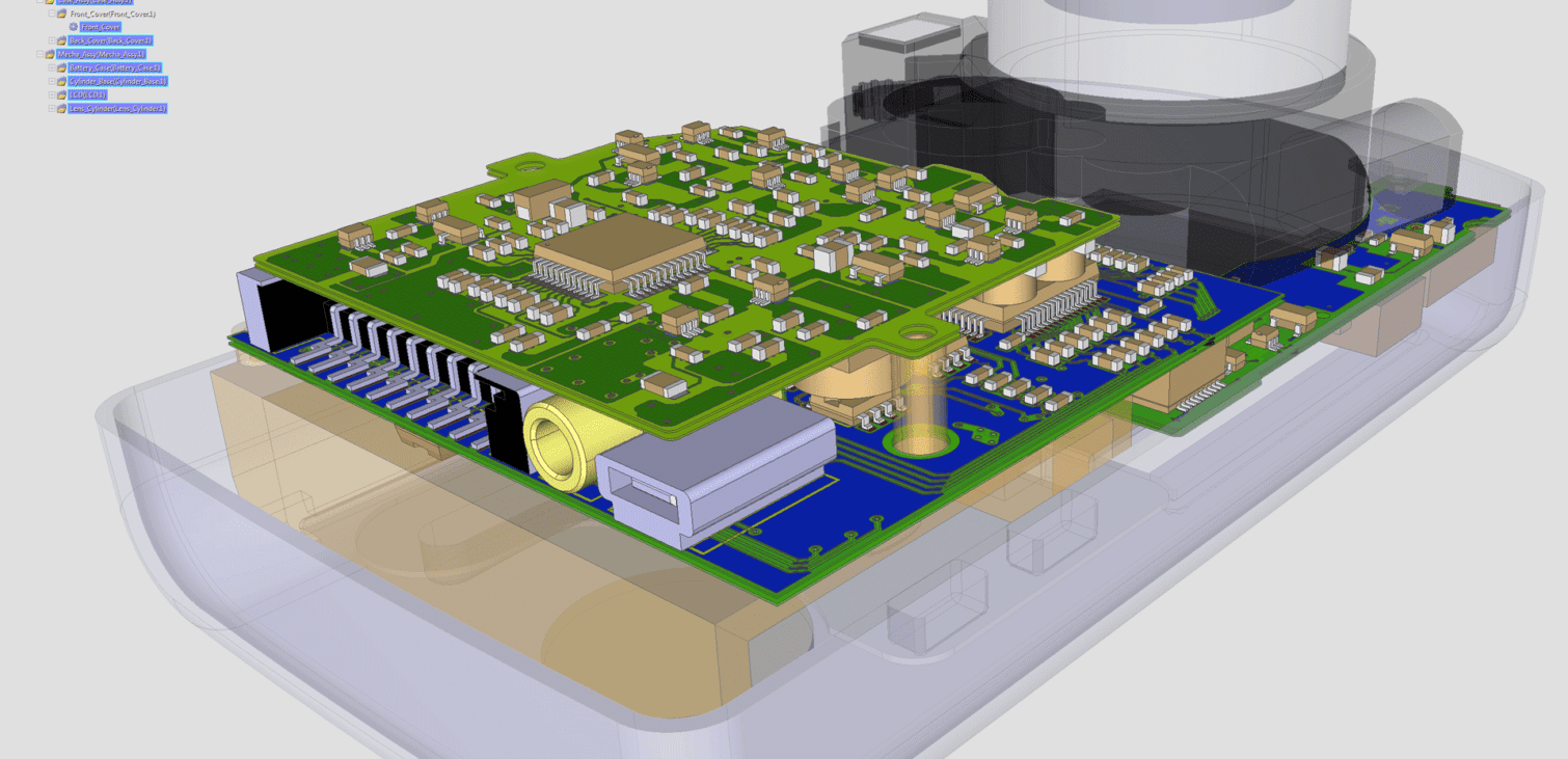
Design Force lets you manage multiple boards in one system, and bring them together in their physical environment.
Design Force combines traditional 2D PCB design with native 3D multi-board PCB design to support single board, multi-board, and chip-package-board analysis and optimization.
PCB designers can manage multiple boards in one system and select a combination of PCBs, packages, and SoCs. In other words: you can complete the layout of your design as a complete system.
Design Force is the industry’s only chip/package/board co-design solution in one design tool.
With Design Force you can design and optimize your IC packaging design and, in fact, never leave your PCB layout.
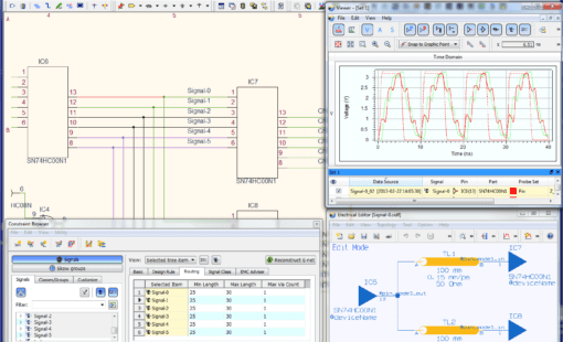
Design Force supports advanced PCB layout tasks with sophisticated manual and automatic features that adhere to a configurable set of constraints. Built-in analysis tools allow users to conduct signal integrity analysis concurrently during the physical layout.
Easy-to-use interactive placement and routing features along with powerful auto-placement and auto-routing capabilities boost productivity while automatically adhering to constraints. As a result, Design Force can ensure manufacturability and signal as well as power integrity.
Our multi-board PCB design software allows access to embedded EMI and power integrity analysis. It also supports integrations to best-in-class analysis solutions for disciplines such as RF, Full-wave 3D signal integrity, power integrity, and thermal.
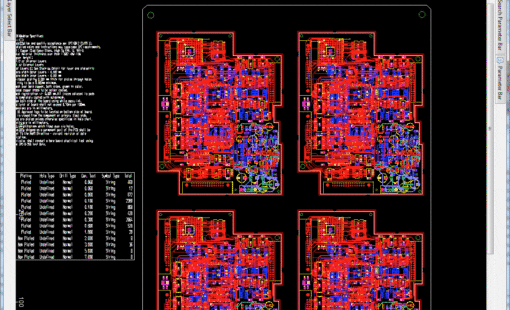
Design to any manufacturing specification during layout with built-in design for manufacturing (DFM) checks. Creation of panel designs, fabrication and assembly drawings, and CAM outputs.
CR-8000 Design Force allows for a multitude of extensions to meet your specific design requirements
CR-8000 ADM (Advanced Design for Manufacture) facilitates comprehensive checking of PCB manufacturability early in the design process. In essence, the checks assess whether the design conforms to manufacturing as well as component mounting specifications.
As IC packaging architecture advances, Design Force enables the designer to deal with the growing complexity in design space especially in handling high pin-counts, high-density designs, and the need to interface with multiple formats and flows.
With this purpose in mind, parametric wizards are available to define and optimize pin maps. A native 3D interface is available to deal with the various package architectures allowing for seamless co-design with chip and PCB designs. For feasibility studies, automatic fan-out and full routing features are available.
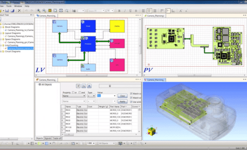
Our PCB layout software offers true co-design through a hierarchical setup that can bring multiple designs together in the same framework. The connectivity between designs can be set up automatically or manually.
In either case, the user is then able to move between designs (chip RDL, package, or board, or any combination thereof). This enables the user to accurately see and edit the nets/routing on a system scale.
A powerful PCB FPGA co-design environment that enables the exchange of I/O and constraint information between PCB designs and FPGA designs.
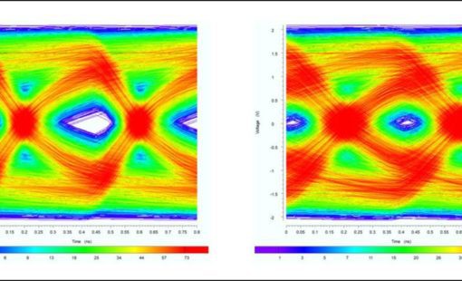
Scenario EX enables checking the electrical characteristics and the connection topology of signal tracks. For instance, it allows “What-If Scenarios” of both schematic and layout data to optimize the behaviour of a circuit. It can be used both for interactive design and design verification. Scenario EX can be used either stand-alone or embedded into Design Force (Design Force SI).
CR-8000 includes fully-integrated simulation and analysis tools to verify all aspects of your single or multi-board designs including:
Fast and easy check of the current density of a layout structure towards a given maximum.
Designers can specify multiple instances of strategy-driven areas and simultaneously auto-route the design.
Board Viewer – free CAD viewer
Board Viewer allows users to share and review native Design Force data to enhance overall communication during product development.
Board Viewer Advance
An enhanced viewing tool for sharing and reviewing Design Force design information. Including component property viewing (query), cross-probing with schematics; Design Rule Checks and manufacturing rule checks; graphical comparison of boards.
3D product visualization is unquestionably becoming a critical need as electrical and mechanical designs converge with little room for error. Many companies cite ECAD / MCAD design synchronization as a significant product design challenge. Traditional 2D PCB-centric design evidently cannot meet the needs of a 3D multi-discipline product design process.
A simulation environment for Power Integrity (AC impedance and de-coupling impact, DC voltage drop, current analysis) and electro-magnetic interference (EMI) with attention to full board screening, differential mode, common mode, power bus noise).
An extension to Design Force specifically for the creation of panel designs, fabrication and assembly drawings, and CAM outputs.
Our satisfied customers
Related Resources
Find out more about CR-8000 Design Force via our blogs, press releases and more...
On-demand webinars
Using the example of the analysis of SerDes transmission paths such as PCI Express, SATA or USB3, we explain the methodology of an analysis- and constraint-driven assembly development with CR-8000 Design Force.
With its support of 3D, CR-8000 Design Force offers the possibility of validating PCB designs against the mechanical envelope. In this session you will learn how to use formats such as IDX and JT in Design Force or, alternatively, how to import native 3D data from various MCAD systems.
This webinar will introduce the use of the Ansys Electronic Database (EDB) format to share information from CR-8000 Design Force to Ansys, the advantages beyond the former ANF-based interface, and how this can help users be more effective and productive.
The typical design flow for a power module is in MCAD, where only structural analysis is possible. Moving to a new design flow using CR-8000 Design Force also allows for electrical analysis too. This webinar will demonstrate the features and benefits of this new design flow.
Design Force Blog Posts
Discover how CR-8000 and Polar Speedstack™ enhance high-speed PCB stack-up design by optimizing impedance control and manufacturability for improved performance.
Wireless Power Transfer (WPT) is replacing cables and wires in consumer electronics, electric vehicles (EVs), and healthcare. Zuken offers a suite of solutions that help engineers design, simulate, and validate WPT systems. Learn more.
A trend towards low power design prevails in the electronics industry today and is not likely to change in the near future. This development is driven by many reasons but primarily by the performance and storage density demands of mobile devices, where a reduction of the power consumption is crucial to extending battery life without sacrificing the bandwidth. This comprehensive guide helps you mitigate LPDDR4 Design.
Back drilled vias: Save cost on buried vias and control cross talk.
Related Products
CR-8000 Design Gateway provides a platform for logical circuit design and verification of multi-board system-level electronic designs.
System Planner provides a system-level design environment for the architectural planning and optimization of electronic systems and products.
With a robust set of features for data preparation and embedded verification to verify manufacturing specifications, DFM Center addresses the challenges of the manufacturing process.
DS-CR supports the specific demands of PCB design data management. It combines multi-site library, design data, and configuration management capabilities into a unified engineering environment.