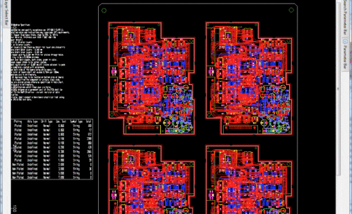
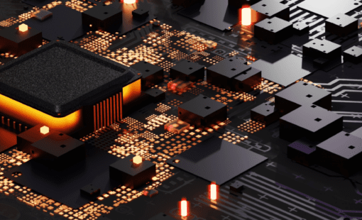
PCB system architecture design

Zuken’s CR-8000 is the most advanced PCB design software in the industry with architecture design and verification, multi-board PCB layout with MCAD integration, SI/PI analysis, and chip/package/board co-design. CR-8000’s PCB design tools simplifies your most challenging PCB subsystem designs.
CR-8000's end-to-end integrated design flow extends from initial system planning, where fundamental decisions are made about partitioning, component selection, form, fit and function of the product or system, through the creation of detailed schematics and layout of single and multi-board PCB systems, to manufacturing optimisation. A modular, object-oriented architecture ensures consistency of all data and versions from concept to production.
PCB system architecture design

Partition complex systems into multiple connected PCBs

Manage IC, package and PCB in one single environment

Control releases, revisions, and configurations with integrated data management
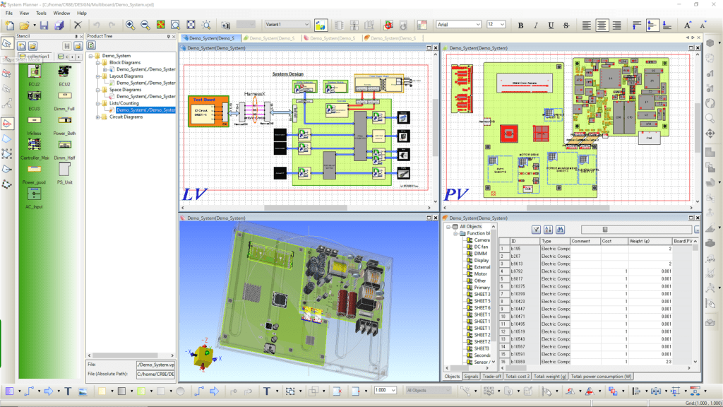
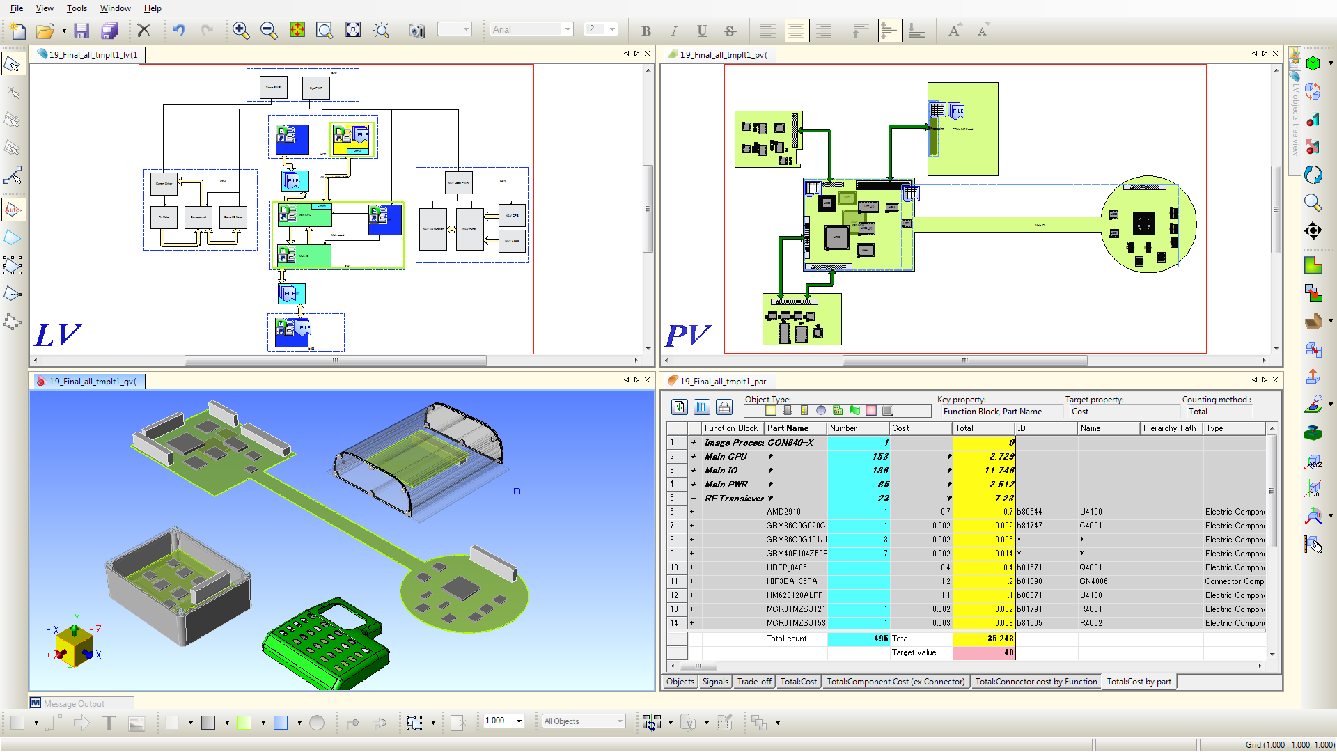
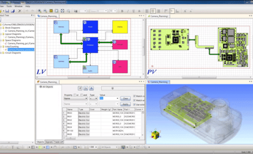
CR-8000 System Planner is the industry’s only PCB system architecture design and verification tool that is fully integrated with detailed PCB and wire harness design. As products become more complex, optimizing the architecture is more critical than ever.
System Planner combines four disciplines into one design and analysis experience.
The system-level circuit design capability of CR-8000 allows designers to view and optimise the entire electronic system as a whole. With integrated simulation and analysis tools, they can evaluate the system’s performance, signal integrity, current distribution and thermal characteristics. This helps identify and correct potential problems early on to ensure design integrity. In addition, CR-8000 provides powerful design rule checks to ensure that the design meets the specific requirements and standards of different manufacturing sites. These rules are configurable and can cover various aspects such as electrical, mechanical and manufacturing requirements.
Design Gateway
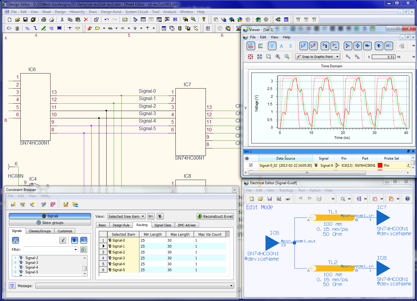
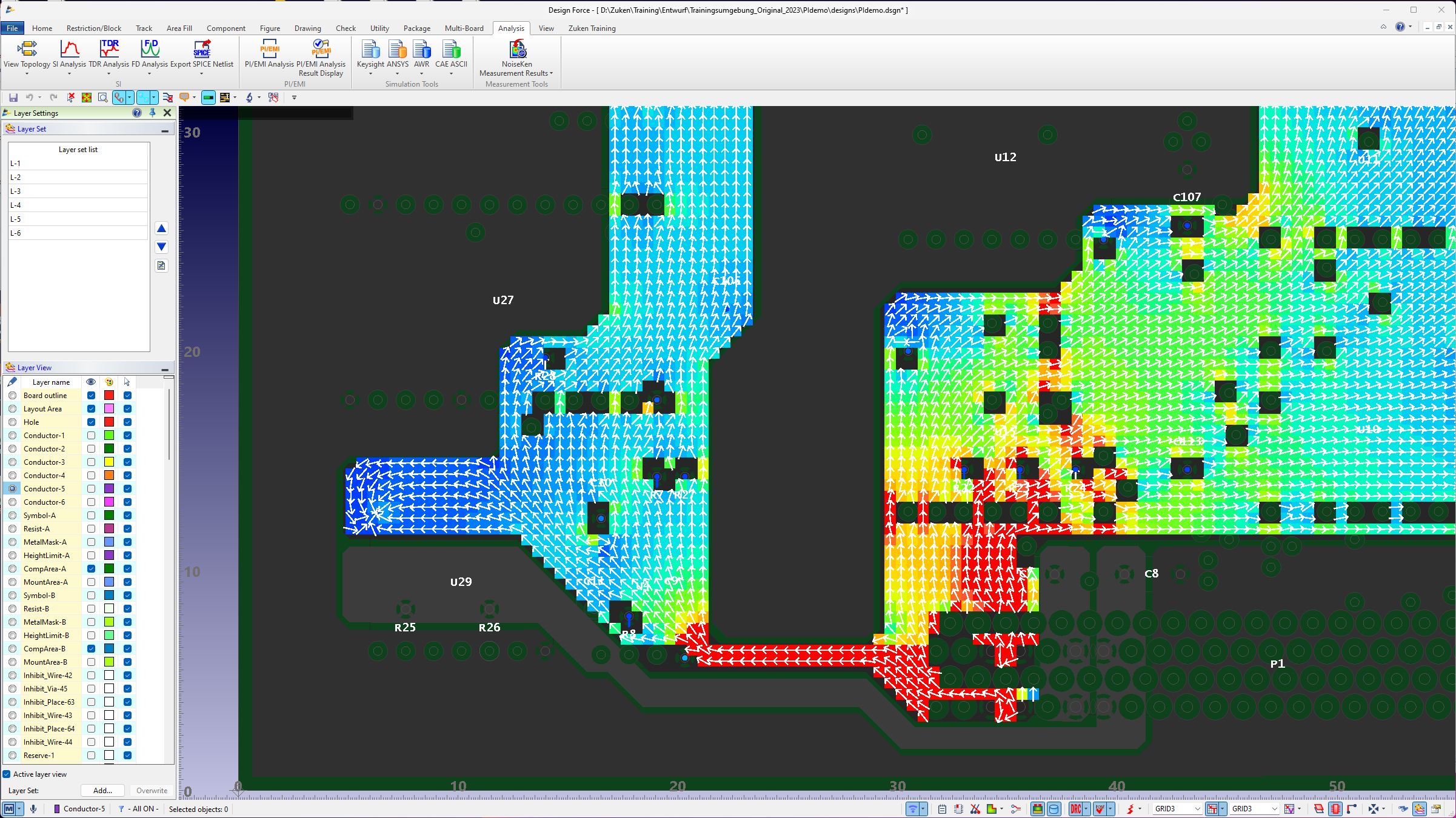
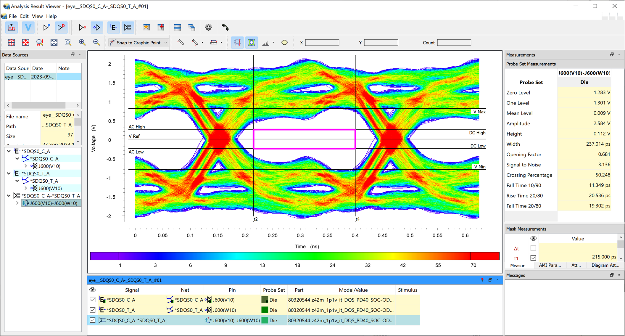
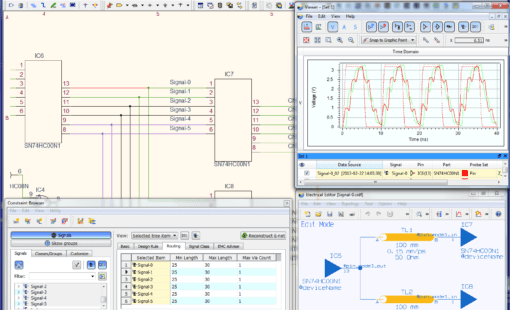
Today’s complex boards or multi-board systems require detailed planning and analysis. With the products Design Force PI/EMI Advance and SI Advance, CR-8000 provides you with all the PCB design tools to build high-speed boards with integrated signal and power integrity analysis with pre-layout planning. Third-party integrations with Ansys and Keysight bring additional capabilities from the industry leaders.
Design Force Advance – Power IntegrityDesign Force Advance – Signal Integrity
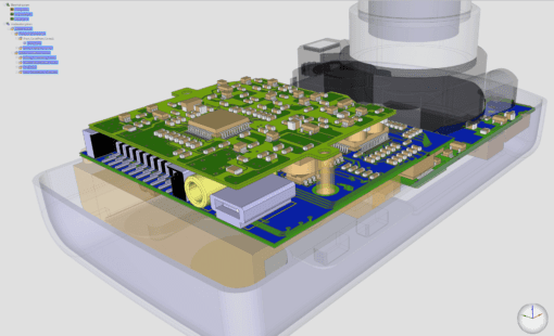
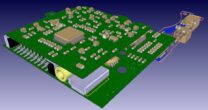
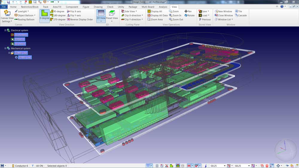
As product complexity grows, the physical layout of a printed circuit board must be considered in the context of the entire system. A PCB system design platform includes support for multi-board design and analysis, MCAD integration, and wire harness design. CR-8000 goes beyond to include chip/package/board co-design.
As companies move to Digital Engineering and model-based design processes, the need for a system design solution is critical. Detailed design teams will be handed a system for implementation, not a PCB. CR-8000 is built for system-level implementation.
Design Force
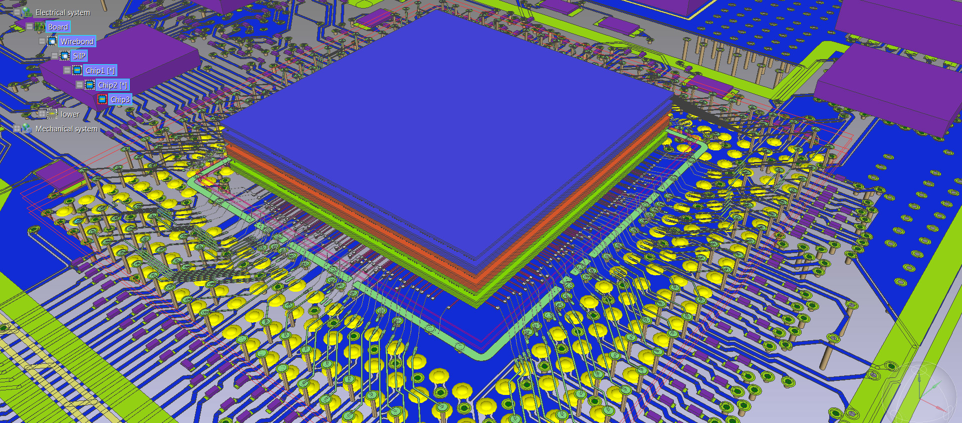
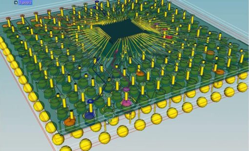
Design Force offers an intuitive, integrated environment for designing single and multi-die packages for wire-bond, flip-chip, and high-density advanced packaging. Designers can start designs with early prototype input of chip and package data from the library, reuse data from IC layout tools, and take advantage of parametric wizards to streamline the creation of the system.
Design Force – IC Packaging
Artificial Intelligence (AI) is an evolving and promising tool in the field of PCB design. Additionally, whether you’re a design veteran or a newcomer, AI offers many benefits that can make your life easier. However, it’s not without its challenges. As technology progresses, the only question is: Are you ready for the AI-driven future of PCB design?
AI in PCB Design


PLM systems are typically not well equipped to manage electronic component libraries and work-in-process data required in the PCB detailed design process. Zuken’s DS-CR provides WIP design data management, design collaboration, project management, design re-use, “where-used” traceability, and much more.
DS-CR is also fully integrated with leading PLM systems for the manufacturing hand-off or component information synchronization. Component information can be automatically synchronized with supply chain partners.
DS-CR
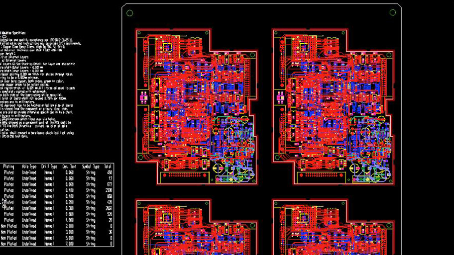
DFM Center enables designers to handle the increasing complexity and diversity of today’s PCBs while ensuring high final product quality, and accurate outputs for the manufacturing processes. With a robust set of features for data preparation and embedded verification to ensure manufacturing specifications are met, DFM Center addresses the challenges of the manufacturing process.
DFM Center
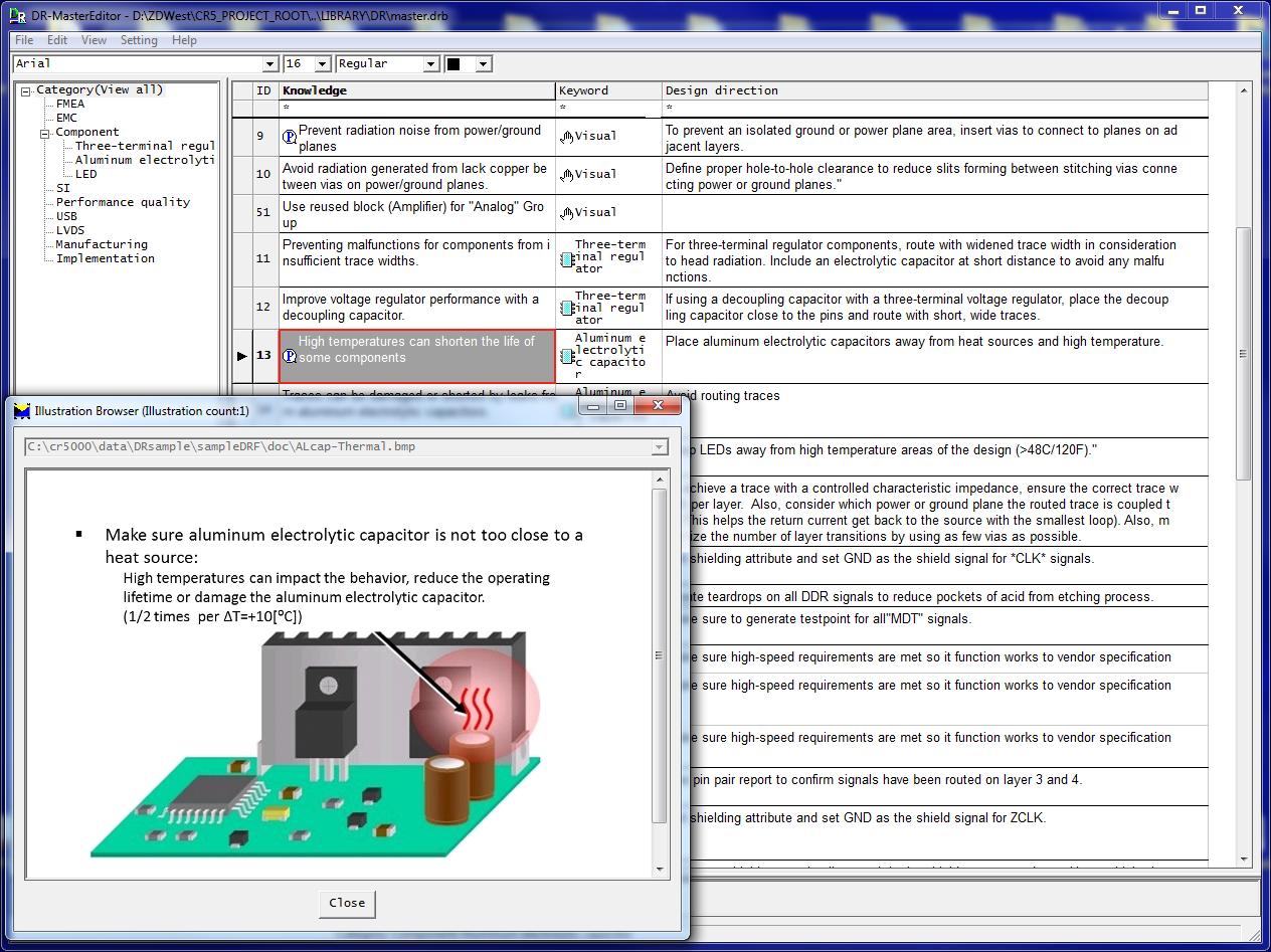
CR-8000 Circuit DR Navi helps design teams consolidate engineering expertise and PCB layout best practices into a central database integrated with the design process. With its comprehensive functionality it is particularly useful to communicate engineering intent and to provide guidance to new members of established design teams.
Circuit DR Navi
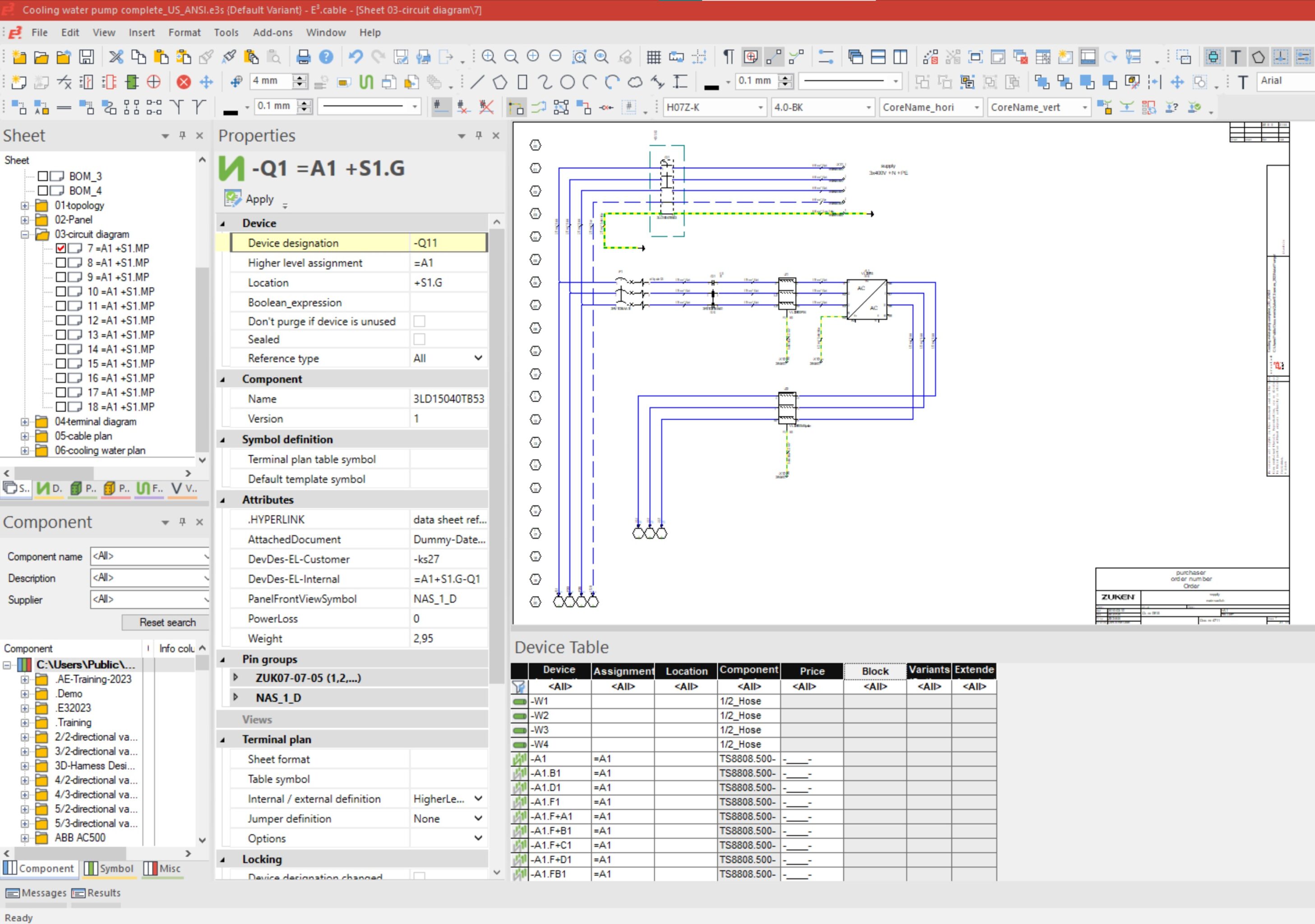
As products get more complicated, the siloed approach to detailed design is missing the mark. As a consequence, wire harness pin assignments are frequently out of sync with the PCB. A system design approach including PCB, wire harness, and MCAD eliminates those common errors. Zuken embraces this approach by using a standard PCB manufacturing output, IPC-2581, to design the wire harness. Zuken’s E3.series imports IPC-2581 directly from CR-8000 PCB design software, eliminating design errors.
E3.series
System Planner provides a system-level design environment for the architectural planning and optimization of electronic systems and products.
CR-8000 Design Gateway provides a platform for logical circuit design and verification of multi-board system-level electronic designs.
CR-8000 Design Force is the fastest, most effective PCB design solution available today. Design Force enables design teams to layout and verify their designs in the context of a complete system or product.
Design Force offers an intuitive, integrated environment for designing single and multi-die packages for wire-bond, flip-chip, and high density advanced IC packaging.
With a robust set of features for data preparation and embedded verification to verify manufacturing specifications, DFM Center addresses the challenges of the manufacturing process.
DS-CR supports the specific demands of PCB design data management. It combines multi-site library, design data, and configuration management capabilities into a unified engineering environment.
Just some of our satisfied customers
Working in safety - this is the value proposition of Pizzato Elettrica, a well-established industrial safety company based in Marostica, Italy, which has chosen Zuken to implement a solution that integrates its electronic design environment with the company's PDM infrastructure.
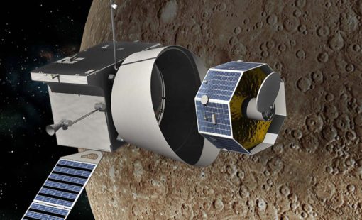
EREMS, a French enterprise specializing in the design and realization of high-tech electronic equipment and of associated software for Space, Defense, and Aeronautics uses CR-8000 and DS-CR from Zuken for the design and lifecycle management of flight electronics, ground electronic equipment, and test benches.
ONTEC faced a difficult challenge: develop a multimedia broadcasting product while complying with a customer’s electromagnetic interference requirements, all within a tight development schedule. ONTEC used Zuken’s CR-8000 with Keysight’s ADS (including SiPro) to meet the requirements of the challenge
A collection of testimonials from satisfied CR-8000 customers
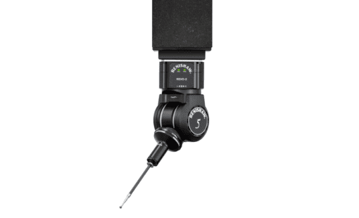
Flexible and flexi-rigid PCBs are integral components within many of Renishaw’s products, and detailed signal integrity analysis is needed to ensure high speed digital signals can be transmitted with minimal distortion. Renishaw migrated to Design Gateway and Design Force, part of Zuken’s CR-8000 PCB design suite, primarily to help with the design and analysis of next-generation flexible PCBs.
With PCB data and process management solutions from Zuken, Endress + Hauser has standardized development and manufacturing processes across five geographically-distributed operations, enabling company-wide parts standardization, design-reuse and increased engineering productivity.
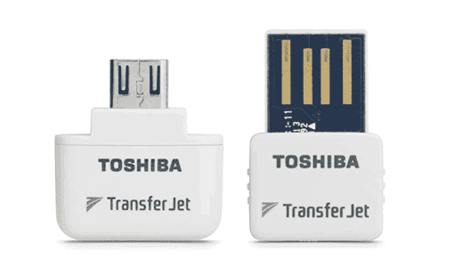
Toshiba faced a difficult design problem: their TransferJet™ technology was embedded in a customer cell phone, and when the next rev of the phone they needed to shrink the board and the module thickness. On top of that, they had to add RF matching to simplify the adoption of the module. Toshiba used Zuken’s CR-8000 Design Force with ANSYS analysis tools to accomplish the project.
CR-8000 Resources
Check out our latest webinars, white papers, blog posts, tech tips & more
Discover how Zuken’s CR-8000/DS-CR integrates with Dassault Systèmes’ 3DEXPERIENCE Platform, providing robust solutions for efficient data management and collaborative workflows between electrical and mechanical design teams.
In this Webinar, you will discover how to streamline your PCB design process with CR-8000, and seamlessly integrate prototype testing results using NoiseKen for enhanced accuracy and performance.
In this Webinar, an optimized PCB design flow combining Zuken CR-8000 technology working tightly with stackup optimization capabilities provided by Polar Speedstack ™ will be presented.
This webinar will demonstrate how Zuken's CR-8000 Enterprise PCB Design System automates updates and redesigns in response to component obsolescence. Learn how to identify affected modules, update designs with a schematic module library, and intelligently assist layout modifications.
CR-8000 Webinar: Zuken recently announced the upcoming release of the industry’s first AI-based PCB place and route product - Autonomous Intelligent Place and Route (AIPR) - This webinar will examine how companies and users will benefit.
Modern electronic products are no longer built around a single PCB. As systems become faster, denser, and more interconnected, engineering teams are being forced to rethink how they design, verify, and manage complex multi-board products.
Explore how CR-8000 enhances PCB design with integrated control of impedance and resistance—enabling precise analysis for both high-speed and high-power applications, from signal integrity to power distribution optimization.
AI in PCB design is increasingly seen as a game-changer, with some predicting it could soon replace entire layout teams—but this view risks overlooking both the current limits of AI and the critical expertise engineering demands. At DesignCon 2025, experts from emphasized that AI's real value lies in complementing human judgment, not replacing it. Read more on our blog.