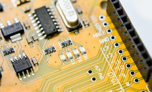
Back drilling vias: Save cost on buried vias and control cross talk
Back drilling vias is a cost-effective alternative to buried vias in multi-layer board manufacturing. While blind and buried vias require separate drilling and plating operations for the related inner layers, it is certainly a cheaper alternative to simply drill and plate through all layers of a multilayer board.
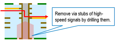
The downside of this approach, however, is represented by undesirable antenna and cross talk effects that will be caused by the unconnected parts of the vias at elevated clock speeds. To eliminate these parasitic effects, the unused via stubs need to be drilled out to a defined depth during the final phase of board production. This process is referred to as back drilling.
How to define back drilling parameters in CR-8000 Design Force
With CR-8000 Design Force from Zuken, the back drilling of vias is no longer an afterthought during board production. It becomes an integral part of board design. And here is how it works:
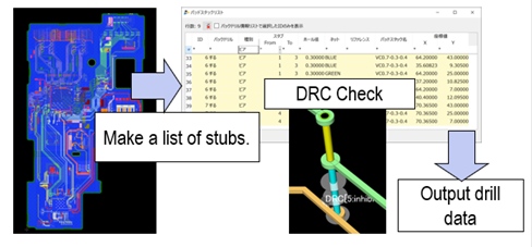
- Set back-drilling conditions: Define the maximum admissible stub length in the rule editor of CR-8000 Design Force
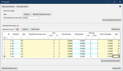
- Extract pad-stack and define drill hole specifications
- Specify drill diameter and drill layer in back-drill information list
- Output drill data
These and more features are all part of the release 2020 of Zuken’s CR-8000 3D multi-board design tool suite.


- Blog
Discover how CR-8000 and Polar Speedstack™ enhance high-speed PCB stack-up design by optimizing impedance control and manufacturability for improved performance.
- Blog
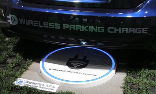
Wireless Power Transfer (WPT) is replacing cables and wires in consumer electronics, electric vehicles (EVs), and healthcare. Zuken offers a suite of solutions that help engineers design, simulate, and validate WPT systems. Learn more.

- Blog
A trend towards low power design prevails in the electronics industry today and is not likely to change in the near future. This development is driven by many reasons but primarily by the performance and storage density demands of mobile devices, where a reduction of the power consumption is crucial to extending battery life without sacrificing the bandwidth. This comprehensive guide helps you mitigate LPDDR4 Design.
- Blog
Checking for potential electromechanical collisions is usually done more in the mechanical design environment. However, shifting the check to the electrical side during component placement can help create a more robust product. For multi-board PCB design, there are several built-in checks in Design Force that validate the design for collision and clearance requirements.
- Blog
Discover how CR-8000 and Polar Speedstack™ enhance high-speed PCB stack-up design by optimizing impedance control and manufacturability for improved performance.
- Blog
Wireless Power Transfer (WPT) is replacing cables and wires in consumer electronics, electric vehicles (EVs), and healthcare. Zuken offers a suite of solutions that help engineers design, simulate, and validate WPT systems. Learn more.
- Blog
A trend towards low power design prevails in the electronics industry today and is not likely to change in the near future. This development is driven by many reasons but primarily by the performance and storage density demands of mobile devices, where a reduction of the power consumption is crucial to extending battery life without sacrificing the bandwidth. This comprehensive guide helps you mitigate LPDDR4 Design.
- Blog
Back drilled vias: Save cost on buried vias and control cross talk.