Checking for potential electromechanical collisions is usually done in the mechanical design environment. However, shifting the check to the electrical side during component placement can help create a more robust product. For multi-board PCB design, there are several built-in checks in CR-8000 Design Force that validate the design for collisions and clearance requirements. In the third and final part of this multi-board design series, I’ll explain how the front-loading of this validation process works.
In part 2, we created and validated a system circuit diagram. Now it’s time to move on to the layout, passing the design from Design Gateway to Design Force.
First of all, a Design Force Configuration File must be created. This is, essentially, a type of system netlist that contains the description of the linked boards and the net names of the interconnected connectors. With this file, the configuration can then be imported into Design Force and no additional setup is necessary. In Design Force, the individual boards can be further edited at any time.
With the Mechanical Object Organizer, the routed boards can be linked to mechanical objects. Usually with STEP files, but also other native files, for example from Catia, SolidWorks, Creo or Siemens NX can be imported.
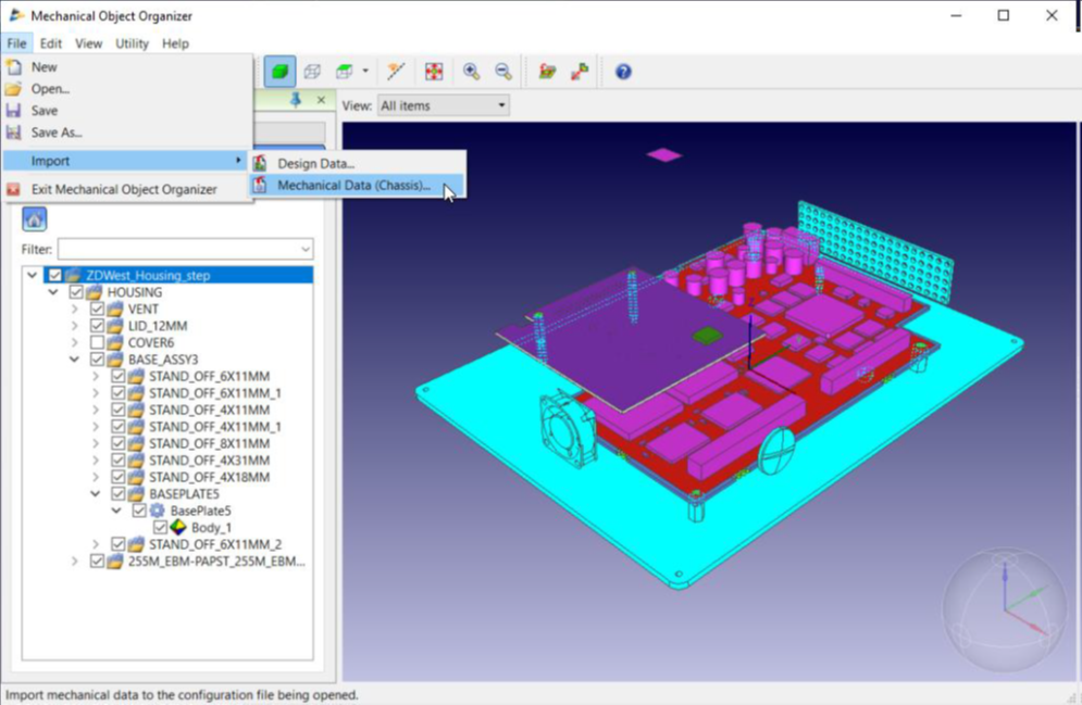
As soon as the import is complete, the mechanical objects are listed in the Design Tree View. For a better overview, individual objects can be shown or hidden and also deleted respectively. Once the alignment is complete, this system configuration can also be opened in Design Force. Various checks can now be run in the 3D PCB design workspace.
Collision Course
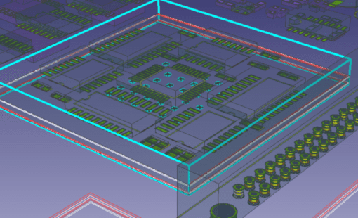
The Collision Check tests various objects for collision. The Collision Check Settings can be configured to define which objects are tested: Board Outline, Component, Height Limit Area, or mechanical data. If an Accurate Shape Part has been assigned to individual components, for example, a connector or a STEP, the checks can be targeted at this Accurate Shape Part.
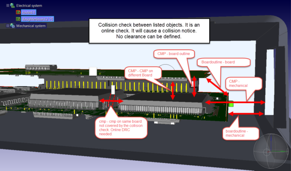
The Collision Check can be performed on any selected objects or on an entire system. The user can display the error objects contained in the collision check report and then cross-probe in the system.
Which objects can the Collision Check validate?
- component and component on different boards
- component and board outline for the different boards
- board outline to board outline
- component to a mechanical object
- board outlines to a mechanical object
The Collision Check does not replace the regular Design Rule Check though, because it will check objects between different PCBs and the package, but not components on the same PCB.
Clearance checks in the 3D workspace
The 3D Clearance Check not only scans for a collision but also checks objects against a defined clearance. The clearance rules can be defined precisely for a PCB and saved to be used for other PCBs in the future.
The resulting 3D Clearance Check Report lists all errors in the system. Again, there is the possibility to cross-probe in the system, communicate, and display the error. This way a whole system can be validated based on the clearance between different objects.
Which objects can the Clearance Check validate?
- package to component
- component to board outline (of the second board)
- component to component with a set clearance between the boards, also applicable to flex-boards
- board outline to a mechanical object
- clearance of the nets between the boards
- net to package (net to net is validated with the regular design rule check).
Considering the overall system, this check could be very helpful and save a lot of work, especially eliminating loops between mechanical and electronic design.
See also:
- CR-8000 Design Force: 3D Multi-Board PCB Design Software
- Webinar: 3D PCB Multi-board Design Basics
- Whitepaper: 3D Convergence of Multi-board PCB and IC Packaging Design
- PCB Design in Context
- Blog
The benefits of developing all boards of a system concurrently on a single CAD canvas. Stacking PCBs, as opposed to connecting with cables, in multi-board design is a current and highly popular trend, as manufacturing costs are reduced and reliability improved.
- Webinar
- Products
CR-8000 Design Force is the fastest, most effective PCB design solution available today. Design Force enables design teams to layout and verify their designs in the context of a complete system or product.
