FPGA und pcb co design

FPGA/PCB Co-Design

FPGA Pin Optimisation
Menu


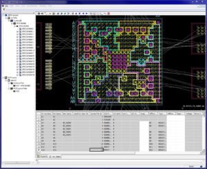
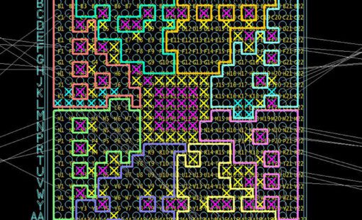
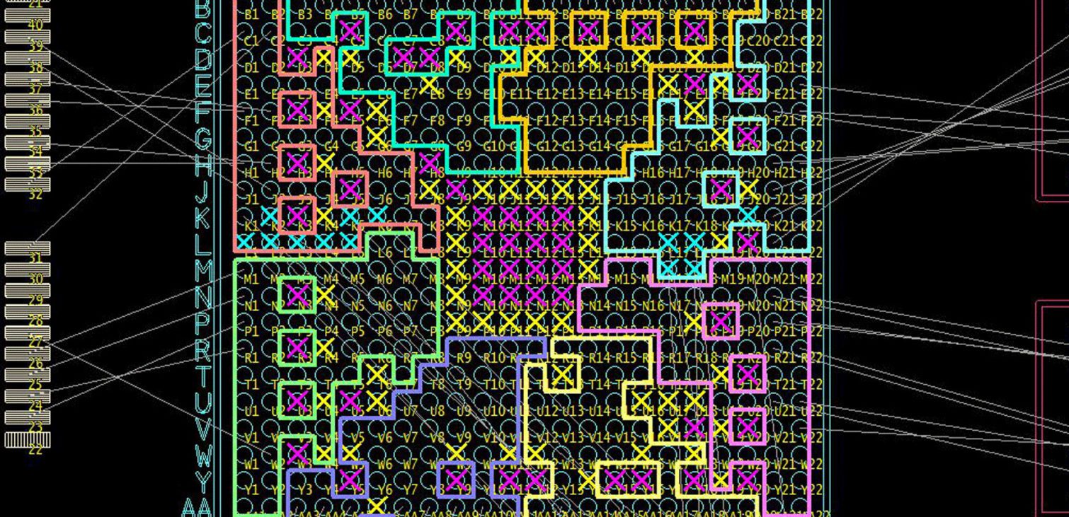
CR-8000 Graphical Pin Manager

Zuken’s Graphical Pin Manager offers an effective FPGA/PCB co-design environment providing support for the latest devices offered by FPGA vendors, such as Xilinx, Intel, Lattice, and Microsemi.

As part of the CR-8000 family, Graphical Pin Manager enables design teams to communicate I/O and constraint information intelligently for FPGAs or other high-pin count devices, at any time, using Design Gateway and Design Force. This means programmable devices can be developed in parallel to the PCB design, and are ready to meet project delivery and production schedules.

Product Features

FPGA designers and librarians can import pin assignment information directly from design suites such as Intel Quartus II, Xilinx ISE Design Suite, Microsemi Libero SoC Design Software, Lattice + ispLEVER/Diamond and Aldec Active-HDL.

Alternatively, BSDL, VHDL/Verilog or CSV files can be used. Graphical Pin Manager also offers an extensive library of FPGA vendor device kits for Intel, Xilinx, Microsemi and Lattice, providing additional key attributes for I/Os, such as differential pairs, pin type, I/O bank and power/ground assignments. Zuken offers up-to-date device kit downloads from our website to access the latest devices from vendors.

FPGA programming and PCB co-design

Once part information is loaded into Graphical Pin Manager, users access easy-to-use wizards to automatically divide and generate symbols for immediate use in logical circuit design. Graphical Pin Manager is also integrated with the library, so users can easily associate the required physical footprints and export directly to the library for fast part creation. Once the pin assignment is defined in Graphical Pin Manager, the pin report file is exported to the FPGA design tools.

As the initial FPGA is simulated and synthesized, engineers can load the logical and physical circuit design within Graphical Pin Manager. Engineers may review the current pin assignment and each of the constraints and rules associated with each I/O, then use the extensive set of utilities to visualize the FPGA on the PCB. The FPGA can be viewed with colored I/O banks, or as the sub-element model defined when dividing the component. This means analyzing the structure and identifying how interconnects relate to other components is straightforward.

FPGA/PCB Co-Design

Graphical Pin Manager also provides a ratsnest view of the board, showing the connection between pins and from partially routed signals. For rules-driven optimization of the I/Os, users can conduct pin swaps interactively, using visual indicators to highlight the candidates for swapping with the selected net. The automatic pin assignment optimization feature then untangles the ratsnest for the selected FPGA components.

Got a Question? - Contact Zuken today

For more information on how Zuken can help your design process, contact Zuken today.
Contact us today