
Are You Making the Most of Modular PCB Design With Design Reuse? - Part 1
Introduction to Modular PCB Design
In this two part series of blog posts, I’m going to be looking at reuse with modular PCB design, and how you can streamline your methodology to reduce design time, reduce design errors and increase product quality.
The electronics industry has been doing it for decades. Software development too.
Although we’ve been talking about it for years, in PCB design it has yet to catch on in quite the same way despite there being a host of benefits to be reaped from modular design practices. So in the first of this two-part series I’d like to challenge you to ask yourself a few questions about how you reuse designs:
- Are you reusing as many of your designs as possible?
- Are you getting some benefits from reusing designs… but inadvertently creating new problems?
Some of the benefits of reusing PCB modules for common functions, include:
- Avoiding potential signal integrity or thermal problems by using circuit data with proven performance.
- Reduction in time taken for schematic capture and PCB design leading to reduction in development costs.
- Fewer design errors.
- Ultimately, helping bring quality products to market faster.
Circuit Design Issues
In fact, efficient reuse is one of the key methods that companies are leveraging to become more competitive and keep up with the volume and frequency of new product introductions. The key word here is ‘efficient’. You maybe reusing some elements of your designs, but it’s being able to do it effectively that’s going to increase quality and improve your development process.
Reuse is getting more attention because much of the electronic content in electronics products has been commoditized, increasing amounts of functionality becoming consolidated in application processors or system-on-chips (SoCs) and their reference designs. Standardization of busses and protocols allow for even more reuse. Other factors include:
- Proliferation of electrical constraints.
- Stricter-than-ever requirements to maintain reliability.
- Manufacturability and compliance.
- Challenges using IC and field-programmable gate array (FPGA) for high-speed design.
Current Circuit Reuse Methods
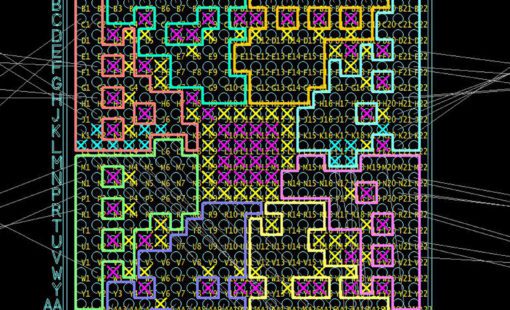
When you need to produce a related product you might often copy and modify the original design, or use predefined modules from the original design. For example, a new cell phone variant might reuse the baseband, Bluetooth and Wi-Fi modules, combined with a new RF section.
But you can run into some potholes with this approach.
The Perils of Human Data Managers
In larger design teams, it can often be difficult to find a related design that fits the specific requirements of the current project, it’s a classic case of you can’t see the wood for the trees – sound familiar? There’s always the potential for the designer to inadvertently reuse a version of a related design that doesn’t include the latest changes.
Other issues that the cut and paste method can lead to include:
- Knowledge developed in creating the original design is typically lost. The copied blocks lack intelligence such as the underlying design methodology and best practices.
- Traceability – sometimes only one person knows the source of individual modules, so if a problem is discovered later on the designers of the new module may not even be aware of the change. The original error will be replicated and there’s the risk it may not be caught before the product is released, or that large costs are incurred by late-stage design changes.
Ouch, these kind of problems hurt. So now we’re on the same level, you know I’m with you there understanding the pain, I’m afraid I’m going to keep you hanging on a little longer, for the answers in part 2, where I look at methods for managing circuit modules, design best practice, and an example of streamlining the product design process.
In the meantime you might like to check out Zuken’s Design Force PCB design software.
Back soon…next week is my deadline, so I won’t keep you dangling for long.


- Blog
Discover how CR-8000 and Polar Speedstack™ enhance high-speed PCB stack-up design by optimizing impedance control and manufacturability for improved performance.

- Blog
Wireless Power Transfer (WPT) is replacing cables and wires in consumer electronics, electric vehicles (EVs), and healthcare. Zuken offers a suite of solutions that help engineers design, simulate, and validate WPT systems. Learn more.

- Blog
A trend towards low power design prevails in the electronics industry today and is not likely to change in the near future. This development is driven by many reasons but primarily by the performance and storage density demands of mobile devices, where a reduction of the power consumption is crucial to extending battery life without sacrificing the bandwidth. This comprehensive guide helps you mitigate LPDDR4 Design.

- Blog
A modular product approach is an established way of improving the calculating and realizing the value of investment goods. Yet modular product initiatives often fail to live up to expectations because of poor coordination between engineering disciplines. To deliver on the promise of a modular product architecture strategy, companies need to create a number of prerequisites in organization, process, and infrastructure.
Related Content
- Products
Graphical Pin Manager offers an effective FPGA / PCB co-design environment providing support for the latest devices offered by FPGA vendors

- Solutions
- Products
CR-8000 Design Force is the fastest, most effective PCB design solution available today. Design Force enables design teams to layout and verify their designs in the context of a complete system or product.

- Blog
In my previous post in this series about effectively reusing design modules to increase product quality and decease development time, I challenged you to think about how well you’re making use of existing design modules and why getting better at this could be a competitive differentiator.