Strengthen high-speed design quality early to avoid rework and achieve reliable layouts without added workflow complexity.
Designing reliable high-speed electronics starts with layouts that support clean signals, stable power, and controlled emissions. As data rates rise and boards become more compact, even small routing decisions can turn into EMC failures or SI/PI violations during testing. EMC Adviser EX gives you a fast, rule-driven way to catch these issues early. It scans your design for the layout patterns that create emissions, degrade signal quality, or reduce power integrity. You get practical insight right on the canvas, without heavy setup or long simulation loops. This helps you build stronger boards and avoid late design surprises.
Strengthen high-speed design quality early to avoid rework and achieve reliable layouts without added workflow complexity.

Apply unified SI/PI/EMC rules to reveal routing, layer transitions, and PDN choices that drive jitter, noise, or radiation.

Detect EMC-critical issues like parasitic antennas, broken return paths, impedance shifts, and high-coupling geometries.
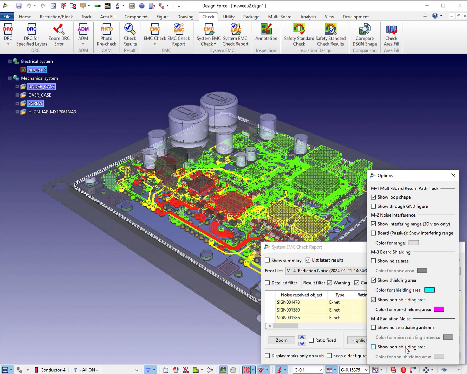
EMC Adviser EX analyzes your design for issues like parasitic antennas, shielding gaps, broken return paths, impedance changes, and high-coupling geometries. These checks help you catch the structures that create emissions, introduce jitter, and reduce noise margins as data rates increase.
The rule set spans SI, PI, and EMC concerns, giving you a clear view of layout risks early in the design. By identifying routing patterns, layer transitions, and power-distribution choices that cause unwanted radiation or signal degradation, the tool helps you build cleaner, more robust high-speed designs without adding complexity to your workflow
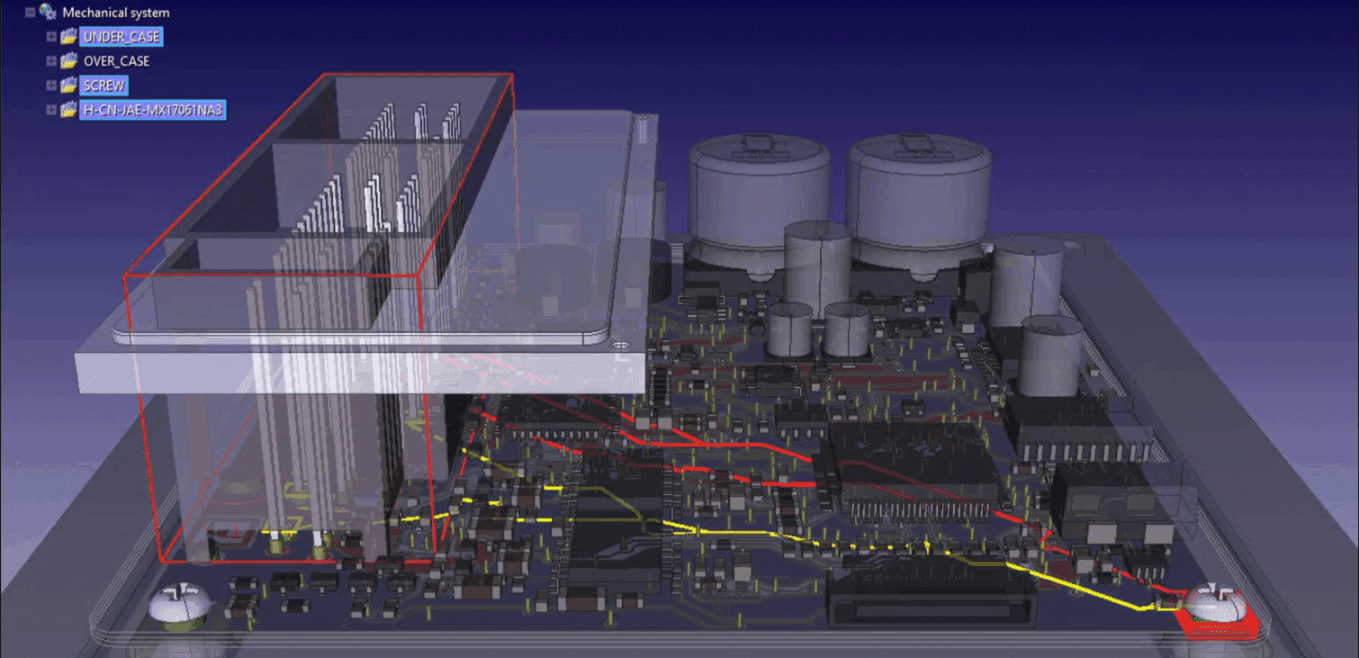
New rules for radiation immunity and stable ground connectivity extend the 3D EMC Advisor beyond emission-focused analysis by revealing how external fields and grounding structures interact with the PCB inside its mechanical enclosure.
By visualizing radiation intrusion, ground-path behavior, and the electromechanical conditions that increase susceptibility, the tool provides early insight into immunity risks that traditional analysis flows do not expose.
EMC Adviser EX delivers analysis that reaches beyond traditional PCB checks by combining electrical behavior with the 3D mechanical context of the product. It identifies parasitic structures, shielding gaps, return-path issues, as well as susceptibility risks driven by external fields and grounding choices. These electromechanical insights appear directly in the layout environment, so teams can validate countermeasures, adjust enclosure features, and refine routing without relying on external solvers or complex model preparation. The result is a clearer view of EMC performance earlier in the design process, allowing
Parasitic antenna checks identify routing and copper geometries that unintentionally radiate at high frequencies, helping prevent emissions issues early in the layout process.
Shielding analysis and rule checks assess the quality and continuity of shielding throughout the design, helping prevent coupling, emissions, and noise intrusion.
Return-path checks verify that high-speed signals use a continuous, low-inductance return path across all layers and boards.
Signal integrity checks evaluate the physical conditions that affect impedance, reflections, timing, and differential-pair quality in high-speed nets.
Crosstalk checks identify routing and PDN conditions that increase unwanted coupling between signals and power nets, on single and multi-board systems.
Power integrity checks verify stable power delivery by evaluating decoupling placement, PDN geometry, connector interfaces, and current-carrying paths.
EMC Adviser EX can be launched from these products
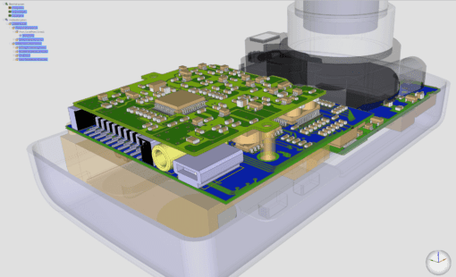
CR-8000 Design Force is the fastest, most effective PCB design solution available today. Design Force enables design teams to layout and verify their designs in the context of a complete system or product.
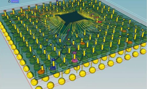
Design Force offers an intuitive, integrated environment for designing single and multi-die packages for wire-bond, flip-chip, and high density advanced IC packaging.
Further reading
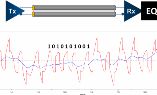
Learn the two key fundamentals for reliable high-speed serial link design and how to overcome signal integrity challenges at multi-Gbps speeds.
EMC problems are often responsible for re-design cycles in PCB design practice. Due to ever shorter innovation cycles of for example cell phones or IoT applications, such as fitness trackers or smartwatches, and many other electronic products, these time-consuming re-design cycles should be avoided under all circumstances.
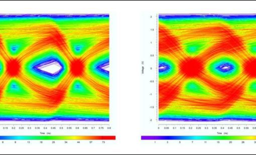
In part 1 of this blog we took a back-to-basics approach and discussed line impedance and its effects in signal integrity. As every electrical conductor comprises capacitance, an inductance, and a frequency-dependent ohmic resistance, and with increasing frequencies, these electrical characteristics will influence and distort the signal.
Related Webinars
In this Webinar, you will discover how to streamline your PCB design process with CR-8000, and seamlessly integrate prototype testing results using NoiseKen for enhanced accuracy and performance.
In this Webinar, an optimized PCB design flow combining Zuken CR-8000 technology working tightly with stackup optimization capabilities provided by Polar Speedstack ™ will be presented.
Using the example of the analysis of SerDes transmission paths such as PCI Express, SATA or USB3, we explain the methodology of an analysis- and constraint-driven assembly development with CR-8000 Design Force.