Mastering Power Integrity: First Get Your Power Distribution System Right
I don’t think I’m generalizing when I say that designers working on complex high speed designs really don’t want to expend a lot of time and effort dealing with power integrity problems. And they especially don’t want to do it using tools that are detached from their design flow. In today’s complex PCBs, we’re talking advanced processors, complex FPGAs and superfast memories, which all share various voltage ranges.
Even though power integrity strategies are now discussed on a daily basis, power distribution design is still a third order design aspect, done late in the design. It involves often a “design-by-hope” approach doing a copper pouring of the power-templates, and additionally sprinkling the board with decoupling capacitors. Such traditional methods of designing complex PCBs, and their power distribution systems (PDS) in particular, cost companies time and money in both the design and manufacturing stages.
But it doesn’t have to be this way
Here is an approach, using Zuken’s embedded power integrity solution in CR-8000 Design Force. The aim is to reduce unnecessary power layers in the board and to eliminate panic approaches, such as adding ‘fear capacitors’. The core concept behind this concurrent analysis solution involves designing the power distribution system (PDS) first to guarantee positive power integrity results as early as possible.
It’s all relative – EMC and the PDS
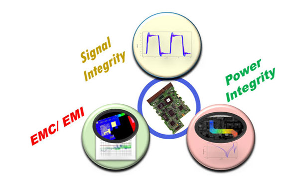
The overall performance and EMC behavior of electronic equipment is not only determined by the design of the circuitry and geometry of the layout, but also by the PDS. Parasitic noise voltages on the power/ground system, caused by the fast switching of currents from integrated circuits (ICs), can lead to malfunctions and significant increases in electromagnetic emissions. High-speed components that utilize numerous complex high-pinout ICs, like FPGAs and CPUs operating on multiple voltage rails, add fuel to the fire.
As these ICs become more of a commodity in electronics applications, the fight for the board real estate required to successfully transmit gigabit-speed signals gets more aggressive. So the traditional approach to address SI, PI and EMC in silos, disconnected from the board layout, is no longer appropriate.
Small changes – dramatic impact
The smallest change in component selection, placement, routing or power/ground plane design can have a dramatic impact on the overall system performance. The PDS is critical. It is a the workhorse of the system providing operational voltage; supplying the current demands of all the active circuits; providing reference levels; implementing the current return paths for all the signal loops; and compensating for external noise. So the PDS needs to be designed rather than created by simply flooding layers with copper.
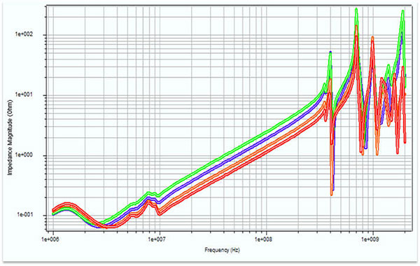
Other issues that reinforce the need to design rather than simply create, include the need to provide charge over a wide frequency range, from low (e.g., system peripherals like disk drives) up to high frequencies, getting into the GHz range. The ongoing lowering of supply voltages and noise margins of today’s ICs make the design of the PDS, and definition of its target impedances, a major design challenge.
Designing the PDS right-first-time
Back when designers only had to deal with a few voltages, there was little need for extensive design to create a PDS. The overall board design process would start with the placement of ICs and routing of regular traces, followed by a definition of the area allocated for the PDS. The final stage in this process was simply to connect all the ICs to the PDS.
The increased complexity and density of boards means that this simple approach is not as effective as it once was. The final stage is no longer just about connecting from A to B; purely because it is no longer physically possible. With today’s complex boards, the approach has been to incorporate different layers for different voltages. But this has a negative knock-on impact on the cost of both design and manufacture. Alternatively, extra ‘fear capacitors’ can be placed on a board in the final stages of design to achieve power integrity. Again, this increases cost in both additional components and manufacturing. The recommended option that eliminates the requirement of extra layers or ‘fear capacitors’, involves designing the PDS first, and then placing the other components around it – ensuring power integrity from stage one.
Effective PDS design
Fast analysis methodology including what-if capabilities for concurrent power integrity analysis is required. Full wave 3D solutions that can provide highly accurate results are unfortunately not applicable within the design process of most electronic systems, where time to market and time to volume are key. A systematic approach that provides design arbitration to achieve a balance between conflicting constraints is essential.
The concept is simple: optimize analysis time invested to achieve reliable decision making results. In order to accomplish this, the new methodology requires that the available data is utilized throughout the design process, and that design consistency is maintained at all levels. EDA tools must manage the various design constraints with the ability to arbitrate between conflicting requirements.
Concurrent design
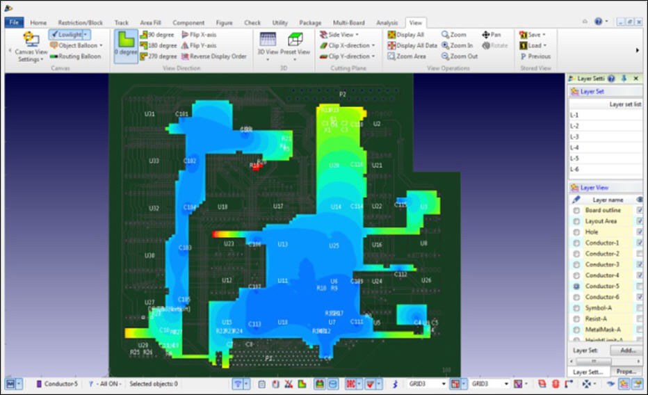
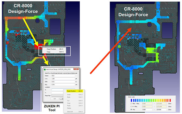
A concurrent design solution, such as Zukens CR-8000, integrates the power integrity methodology into the layout phase of the design process. It also ensures that a consistent set of design constraints, including power distribution and de-coupling requirements, is maintained throughout the design flow. Integrated EMC and power integrity verification is available within CR-8000 Design Force – where constraints conflict, this approach enables them to be resolved early in the design process. Features like adding virtual decoupling capacitors for conducting what-ifs, and parametric studies, and a dedicated solver to compute current distribution and DC voltages, complement the solution.
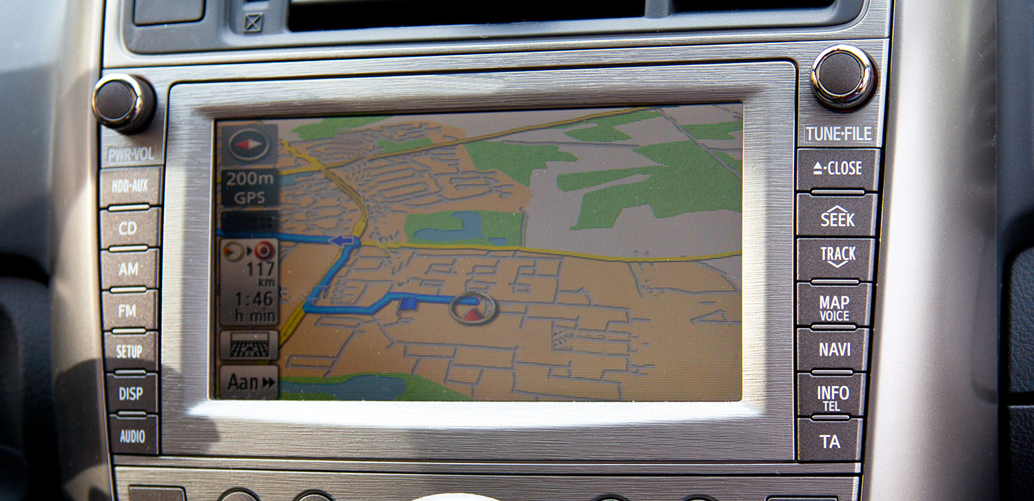
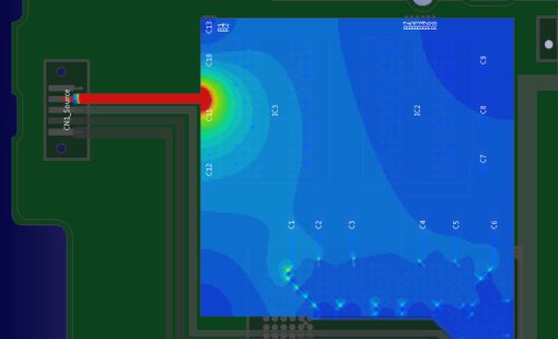
Example – car navigation system
As an example, consider a car navigation system that includes a very small board with a fixed form factor. The unit needs to fit into the radio slot within the car. Boards like these feature high density IC technology such as FPGAs and CPUs, all with fast low power DDR3 (LPDDR3) memories and high-speed data links. The board also has to conform to a set power supply environment defined by the car manufacturer, and must comply very strict EMC limits. The challenge is then to fulfil all these demands to ensure power and signal integrity, and guarantee EMC. The PDS is designed first, and all the components are then placed and routed using the initial PDS design. Just as signal integrity requirements for high-speed systems require designers to organize the topology of connections to achieve clean signals, the architecture of power distribution systems must now be deliberately designed to prevent power integrity problems. But by using advanced design techniques (such as those in CR-8000) and using the concurrent analysis capabilities for SI and PI, costly extra board layers and increased component and manufacturing costs can be avoided.
Find out more about Power Integrity in Zuken’s CR-8000


- Blog
Modern electronic products are no longer built around a single PCB. As systems become faster, denser, and more interconnected, engineering teams are being forced to rethink how they design, verify, and manage complex multi-board products.
- Blog
Explore how CR-8000 enhances PCB design with integrated control of impedance and resistance—enabling precise analysis for both high-speed and high-power applications, from signal integrity to power distribution optimization.

- Blog

- Blog
AI in PCB design is increasingly seen as a game-changer, with some predicting it could soon replace entire layout teams—but this view risks overlooking both the current limits of AI and the critical expertise engineering demands. At DesignCon 2025, experts from emphasized that AI's real value lies in complementing human judgment, not replacing it. Read more on our blog.
Related Content
- Webinar
In our webinar we will provide an introduction to the challenges of signal integrity and the underlying physical effects. This will provide the basis for practical tips to address the related challenges during PCB design.
- Products
CR-8000 includes fully-integrated simulation and analysis tools to verify all aspects of your single or multi-board designs
- Products
CR-8000 Design Force is the fastest, most effective PCB design solution available today. Design Force enables design teams to layout and verify their designs in the context of a complete system or product.

- Products
CR-8000 is a System-Level PCB & IC Package Design software including 3D Multi-board, Analysis and MCAD Integration