Why PCB Design Has Outgrown Single-Board Thinking
A PCIe signal leaves one PCB, crosses a connector, travels through a cable assembly, enters a second board, and suddenly fails EMC testing three months later. The layout on each individual board looked correct. Signal lengths were matched. Constraints passed. Manufacturing files were clean.
But the product still failed.
This is becoming a familiar problem for modern electronics teams because today’s engineering challenges rarely stop at the edge of a single PCB.
Products are now built from interconnected electronic systems — multiple boards, high-speed interfaces, dense packaging, power delivery networks, sensors, embedded processors, and increasingly complex mechanical constraints.
Yet many PCB development workflows still treat boards as isolated design tasks. That gap increasingly leads to integration delays, unexpected redesigns, EMC failures, and rising development costs.
Products Have Become Systems
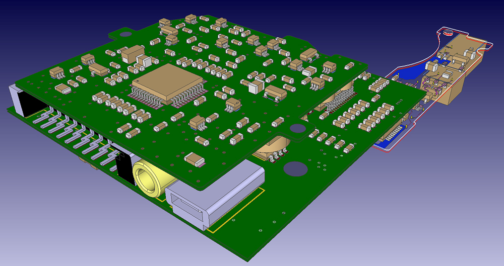
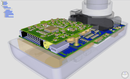
Modern electronic products are no longer centered around one standalone PCB. Automotive systems, industrial equipment, robotics platforms, aerospace electronics, medical devices, and advanced consumer products often contain multiple interconnected boards working together simultaneously.
A single product may include processing boards, power distribution boards, communication modules, sensor interfaces, RF sections, flex circuits, backplanes, and embedded controllers, all working together as part of the same electronic system. Each of these boards influences the others electrically, mechanically, and thermally.
A high-speed signal path may cross several boards and connectors before reaching its destination. A power integrity issue may originate from interactions between subsystems rather than from one isolated PCB. An EMC problem may only appear after the full enclosure is assembled.
The engineering problem is no longer: “Can this board function?”
It is now: “Can the entire electronic system function reliably together?”
The Board-by-Board Workflow Problem
Many PCB development flows were built around individual board ownership. Schematic capture, layout, verification, and manufacturing preparation are often performed separately for each PCB.
That approach worked reasonably well when products were simpler. But increasing system complexity creates problems that cannot easily be identified within isolated board-level workflows.
Interfaces such as PCIe, DDR, Ethernet, USB, and SerDes frequently travel across connectors and multiple PCBs. Engineers may successfully verify trace lengths and routing constraints locally, yet still encounter signal degradation once the complete system is assembled.
Why Engineering Teams Are Shifting Earlier
Historically, many issues were identified during prototyping, integration, or physical testing. As product complexity grows, discovering problems during integration or testing becomes significantly more expensive.
A single EMC failure, signal integrity issue, or enclosure conflict can trigger redesign cycles, additional prototypes, delayed validation, and extended development schedules. That is why many engineering teams are shifting verification earlier in development. The goal is not simply faster PCB layout. It is reducing engineering risk earlier in the product lifecycle.
This shift is changing how PCB development environments are evaluated. For years, PCB software discussions focused heavily on routing productivity, user interface preferences, or isolated feature comparisons.
Those capabilities still matter. But for complex electronic products, they are no longer the whole conversation.
Engineering teams increasingly need workflows that support:
- multi-board development
- visibility into interactions between boards, signals, power, and mechanical constraints
- integrated verification
- electrical and mechanical collaboration
- earlier risk identification
- continuity across the product lifecycle
The discussion is gradually moving away from: “Which PCB tool has the most features?”
toward: “Which engineering environment helps teams develop more reliable electronic systems?”
The Direction of Modern PCB Development
PCB design is evolving beyond individual board layout. As products become faster, denser, and more interconnected, engineering teams are being forced to think at the system level earlier in development.
The challenges that matter most today — signal integrity, power integrity, EMC and mechanical integration — rarely exist on one board alone.
And increasingly, the companies that can identify these issues earlier will have a significant advantage in development speed, product reliability, and engineering efficiency. Because modern electronics are no longer just boards. They are complete interconnected systems.

- Blog
Explore how CR-8000 enhances PCB design with integrated control of impedance and resistance—enabling precise analysis for both high-speed and high-power applications, from signal integrity to power distribution optimization.

- Blog

- Blog
AI in PCB design is increasingly seen as a game-changer, with some predicting it could soon replace entire layout teams—but this view risks overlooking both the current limits of AI and the critical expertise engineering demands. At DesignCon 2025, experts from emphasized that AI's real value lies in complementing human judgment, not replacing it. Read more on our blog.

- Blog
Our new post explores the potential of augmented reality (AR) to transform everyday experiences in shopping, education, and navigation. It highlights how enhanced AR devices will offer immersive, interactive environments that blend the virtual and physical worlds.
More Resoures

- Webinar
CR-8000 Webinar: Zuken recently announced the upcoming release of the industry’s first AI-based PCB place and route product - Autonomous Intelligent Place and Route (AIPR) - This webinar will examine how companies and users will benefit.
- Webinar
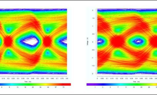
Using the example of the analysis of SerDes transmission paths such as PCI Express, SATA or USB3, we explain the methodology of an analysis- and constraint-driven assembly development with CR-8000 Design Force.
- Products
CR-8000 Design Force is the fastest, most effective PCB design solution available today. Design Force enables design teams to layout and verify their designs in the context of a complete system or product.