
Inside Signal Integrity: Impedance Control – Part 1
Introduction to Impedance Control
Impedance and impedance control are some of the oldest and most discussed topics in PCB design. They are especially important in high-speed design related to signal integrity and power integrity impedance.
In this blog, part one of a two-part series, we’ll go back to the basics of impedance/impedance control and consider what influences line impedance. An in part two, we’ll talk about controlling it.
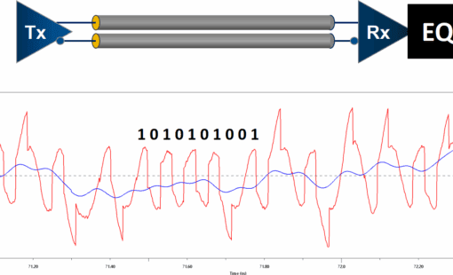
To ensure proper signal integrity for a PCB that incorporates high-speed digital devices, it is essential to control the transmission line impedance.
What do I mean by ‘proper signal integrity’? I refer to signal quality/purity that in the end helps to meet the timing requirements of high-speed digital devices. Increasingly, circuitry features signals with ultra-fast switching times, which must comply with ever-tightening design constraints like skew matching or setup and hold requirements.
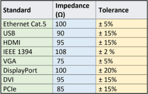
One of the basic constraints – the ‘mother’ of all high-speed constraints, if you will – is line impedance. Be it single-ended or differential (Zdiff). Where high-speed digital ICs are concerned, the OEM or the used standard/protocol will specify the required impedance.
Alternatively, you can try to calculate the desired line impedances yourself. For this, there are a number of formulae that can be used – two of which are shown in figure 2 – that provide varying degrees of accuracy.
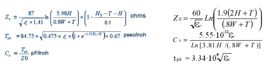
Common to all is that they marry your design elements (e.g., track lengths and widths, layer stacks, etc.) with the physical properties of the intended manufacturing process (predominantly the materials being used). Such formulae can yield esp. for single-ended structures rather accurate results – but there are not suitable for coupled situations (like differential pairs). In that case, more advanced techniques like field solvers are required.
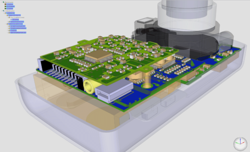
For many PCB designers, dealing with impedance is their first and sometimes only contact with the complex world of high-speed design.
Transmission Line Impedance
The electrical behavior of a signal line is, in principle, dictated by conductor geometry. Once you know the material constants of the surrounding media, you can calculate the dielectric constant, er, which gives the electrical parameters of a line. The trace width, together with the height of the trace, determines the geometry of the trace.
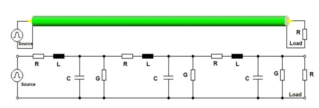
Every electrical conductor comprises capacitance, inductance, and a frequency-dependent ohmic resistance (see figure 1 showing a commonly used electrical equivalent circuit of a transmission line segment). With increasing frequencies, the parasitics and the transmission line impedance cannot be ignored, or it will influence and may distort the signal. As a consequence, the signal becomes an active interconnect instead of a passive connection.
A change in the conductor width always means a change to the cross-sectional area and so has an impact on the maximum current and thermal behavior. In applications where very high clock speeds or data rates, and relatively long electrical line lengths are required (e.g., backplanes), ohmic resistance can also play an important role.
However, the occurrence of a change in the electrical behavior of a conductor through varying its height is relatively rare. Typical multi-layer stack-ups use conductor heights of between 17 and 36μm. These are mainly determined by mechanical constraints, such as the overall board thickness. It should be mentioned that the manufacturing process will deform the ideal rectangular (cross-sectional) shape of the track (etching effect).
Back to the Signal Integrity basics
The characteristic impedance or surge impedance (usually written Z0) of a uniform transmission line is the ratio of the amplitudes of voltage and current of a single wave propagating along the line; that is, a wave traveling in one direction in the absence of reflections in the other direction. Characteristic impedance is determined by the geometry and materials of the transmission line and, for a uniform line, is not dependent on its length.
The standard unit (SI unit) of characteristic impedance is Ohm (W). The characteristic impedance of a lossless transmission line is purely reactive, with no real component. The energy supplied by a source at one end of such a line is transmitted through the line without being dissipated in the line itself. A transmission line of finite length (lossless or lossy) that is terminated at one end with an impedance equal to the characteristic impedance appears to the source like an infinitely long transmission line and produces no reflections. (Source: Wikipedia).
What Does That Mean for a PCB Designer in Terms of Signal Integrity?
It can be shown that an equivalent definition of characteristic impedance is as follows: the characteristic impedance of a line is that impedance which, when terminating an arbitrary length of the line at its output, will produce an input impedance equal to the characteristic impedance. This is so because there is no reflection on a line terminated in its own characteristic impedance (as per the above Wikipedia definition).
The characteristic impedance of a transmission line is determined by the following factors:
- The trace geometry (trace width and height);
- The distance between the signal layer and the current return path; and
- Dielectric constant, εr
To achieve the desired impedance and to match the required tolerances, PCB designers tend to work closely with the PCB manufacturer.
Based on the favored stack-up and the PCB layout demands, a proper impedance calculation method should be chosen. Guesswork and hope are not good engineering practices here, and the impedance targets for at least all critical signals must be determined before routing begins.
In today’s PCB manufacturing processes, tolerances of between 5 and 10% for impedance values can be achieved with: appropriate material selection; proper design of the layer stack structure; trace geometry planning (including any influence the etching process may have), and careful layout.
Summary of Impedance Control
In summary, line impedance plays an even more critical role in today’s high-speed digital designs. Ideally, a transmission line should be terminated at one end with resistance in relation to its characteristic impedance to minimize signal reflections.
In part 2 of this blog, I will discuss how best to achieve line impedance control and outline the ramifications of tolerances in the manufacturing process.
Learn More About Signal Integrity and Power Integrity

-
Product Manager/Senior Consultant


- Blog
High-Speed-Serial-Links wirken oft wie schwarze Magie – steigende Datenraten verstärken dieses Gefühl. Donald Telian (SI Guys) und Ralf Brüning holen die Diskussion zurück zu den Grundlagen.
- Blog
Lerne die beiden wichtigsten Grundlagen für den zuverlässigen Entwurf von High Speed Serial Links und erfahre, wie du Herausforderungen bei der Signalintegrität bei Geschwindigkeiten von mehreren Gbit/s meistern kannst.
- Blog
Der Layer-Stack-up und die präzise Berücksichtigung der Leitungsimpedanz sind entscheidend für robuste High-Speed-Designs. Erfahren Sie in unserem Blog, wie Sie Stack-ups optimal mit CR-8000 und Polar Speedstack™ gestalten können.

- Blog
Die drahtlose Energieübertragung (Wireless Power Transfer, WPT) ersetzt Kabel und Drähte in vielen Bereichen. Die Lösungen von Zuken unterstützen Ingenieure bei der Entwicklung, Simulation und Validierung von WPT-Systemen.

- Blog
In part 1 of this blog we took a back-to-basics approach and discussed line impedance and its effects in signal integrity. As every electrical conductor comprises capacitance, an inductance, and a frequency-dependent ohmic resistance, and with increasing frequencies, these electrical characteristics will influence and distort the signal.
- Products
Sind Sie auf der Suche nach einem Werkzeug, das es Ihnen ermöglicht, die EMV Anforderungen für Ihre Produkte zu erfüllen? Dann ist EMC-Adviser EX genau die richtige Lösung für Sie!
- Products
Integrierte Simulations- und Analysetools zur Verifizierung von CR-8000 PCB-Designs
- Products
Design Force kombiniert konventionelles 2D-Design mit nativem 3D-Design und den neuesten Technologien in Benutzeroberfläche und Grafik für schnellstes Rendern und Aktualisieren.
One Comment