
25 Years of High Speed Design – Looking Back to the Future
It’s 25 years since the first FED Conference took place in Berlin back in 1993, as a gathering for the German-speaking electronic and PCB-related industry. This also happened to be the year we consider as the birth of high-speed design.
I’ve been reviewing my presentation for the anniversary Conference this week, and it’s got me thinking about developments in EDA, particularly in PCB design. We have witnessed such a tremendous technology and design evolution over the past 25 years due to increased design complexity.
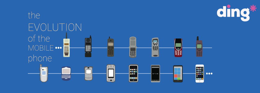
Text messaging is 25
It’s also been 25 years since the first SMS or text message was sent in 1992 (reading “Merry Christmas”). And in 1993 Nokia released its 2110 mobile phone, allowing text messages to be sent and received easily. So the mobile phone is a great marker to help us see how far EDA technology development has come in this time.
Most would agree that mobile phones have seen something between an evolution and revolution, as they’ve become ubiquitous as a commodity and permanent companion. So we can characterize the past quarter century as an electronic technology race – which is also reflected in the way we now design PCBs. It’s an interesting (slightly philosophical) question to ask ourselves whether the progress in the development tools was a catalyst or a trigger for today’s technology. But it’s my view that EDA software, together with the silicon evolution, is one of the key enablers of the amazing technology we now take for granted.
Early days
I’ll be presenting on “High-Speed Design im Wandel der Zeit – 25 Jahre Simulationsunterstützung im PCB-Design” (High Speed Design Changes over Time – 25 Years of PCB Design with Simulation Support”) at this year’s FED Conference. Incidentally, the first event was a small affair with 47 participants and 15 presentations. Since then the conference has developed into a key event with a parallel exhibition, and more than 400 visitors are expected at this year’s event – an indication of growth in the industry.
Here’s a whistle-stop tour of what I’ll be taking about, in case you can’t make it…
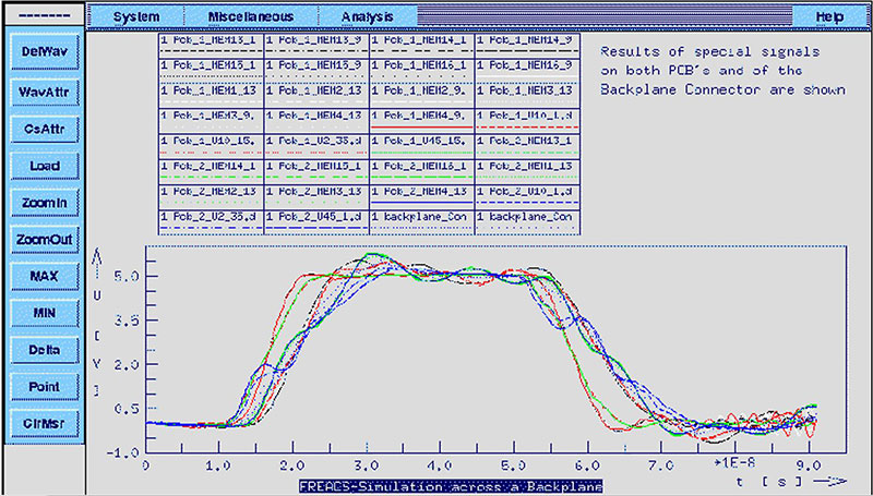
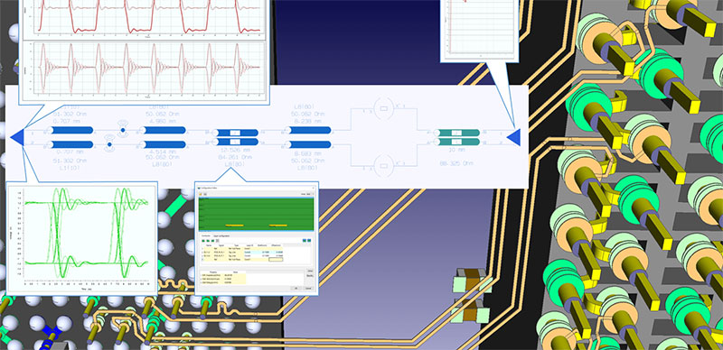
Signal integrity became a serious concern when the transition (rise and fall) times of signals started to become comparable to the propagation time across the board. Very roughly speaking, this typically happens when system speeds exceed a few tens of MHz. At first, only a few of the most important, or highest speed, signals needed detailed analysis or special design care. But as speeds have increased, an increasingly larger fraction of signals need SI analysis and high-speed design practices, including constraining and concurrent validation. In modern (> 100 MHz) circuit designs, all signals must essentially be designed with signal integrity (and power integrity these days) in mind.
In the early 1990s, simulating with respect to signal integrity and high-speed effects (such as quantifying crosstalk or making an accurate determination of transmission impedance) was rather new. SPICE and SPICE-based simulation engines had been in use for a few years, but the main focus of the SPICE simulator (SPICE = Simulation Program with IC Emphasis) developed at UC Berkeley in the 1970s was as a dedicated circuit simulator. And this is still the main application focus of most SPICE derivatives.
Pioneers in SI/PI
For simulating high-speed effects, special modelling capabilities are needed for the high-speed effects caused by fast switching active devices (ICs) – so various special tool vendors developed their own simulation tools as third party complementary add-ons to the PCB design flows.
Quad Design from Camarillo, California and Quantic-Labs from Winnipeg, Canada were simulation tools vendors of that time. Hyperlynx, founded in 1988 (now part of Mentor Graphics) aimed to develop high-speed analysis tools for the PC. INCASES Engineering (founded in 1994 and acquired in 2000 by Zuken) had in mind from the start to enhance PCB design with a complementary concurrent signal integrity simulation, including online impedance calculation and a simulation engine for reflection and crosstalk effects.
The (small at that time) market was dominated by dedicated simulation tools for experts. The simulation processes were mainly post-layout and the tools implemented a kind of virtual measurement facility for selected effects. In most tools, manual processes were required for the calculation of transmission line parameters, or for describing the behavior of the IO-buffers. Automation steps were rare: up to 12 different input files were required for a single SI simulation. Each simulator had its own proprietary IC modelling format, and data extraction often had to be corrected manually (e.g. positive vs. negative copper areas) in the input files.
The IBIS modelling standard was also established 25 years ago in 1993 (what a productive year!) as a common behavioral modelling format for the behavior of integrated circuits, allowing SI simulation to be leveraged in a wider user base.
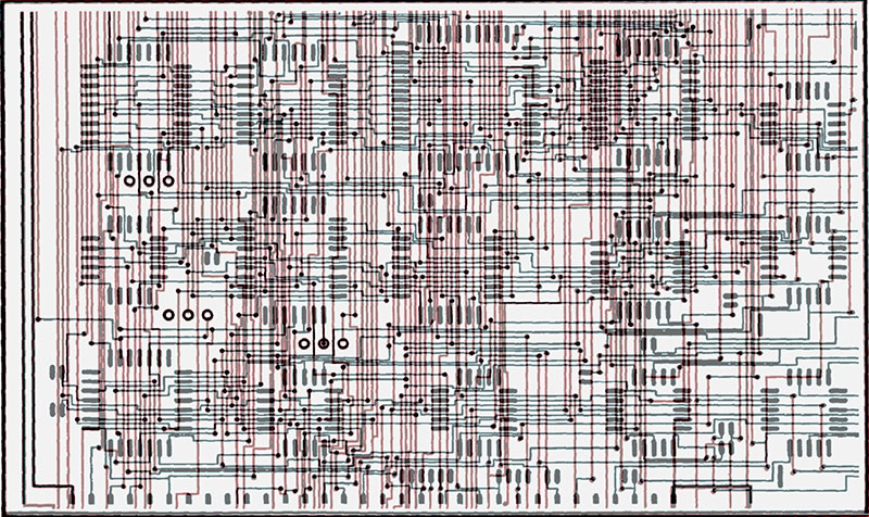
In parallel autorouting and the definition of more complex routing parameters, constraining then became an accepted design methodology. Some of the first attempts were described by Alan Finch and others from Racal Redac in 1985 (Finch, A.c., K.j. Mackenzie, G.j. Balsdon, and G. Symonds. “A Method for Gridless Routing of Printed Circuit Boards”, 22nd ACM/IEEE Design Automation Conference). Meanwhile autorouters – used and judged correctly within their capabilities – are now a cornerstone tool for completing complex PCBs efficiently. Using concurrent autorouting on different areas of the PCB, combined with various strategies and compliance with complex design constraints for high-speed, signal and power integrity, are all key to success.
State-of-the-art
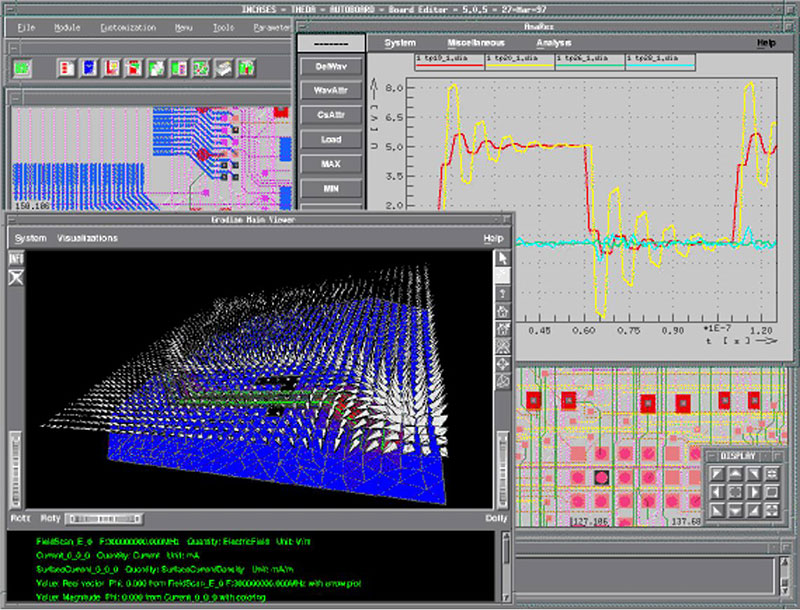
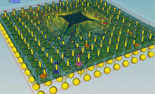
The latest technology for designing tomorrow’s products demands an even more sophisticated approach. Combining traditional 2D design with native 3D design on a multi-board level, including system-level planning, design and concurrent analysis, is the latest PCB design trend. Inherent support for high-speed designs allows engineers and layout designers to conduct signal integrity, EMC, and power integrity analysis concurrently, manage the complex constraints from (multi-board) schematics to the layout process, and autoroute a board – all in a single CAD environment.
With this architecture, designers can effectively co-design a chip, package and board to optimize I/Os at each level, embed components in the dielectric of a stack-up intelligently, and verify manufacturing rules in real-time. They can produce designs with concurrent design-for-manufacturing checks and constraint verification to ensure both manufacturing and engineering intent are maintained during the design process.
It’ll be fascinating to see what the products of the next 25 years demand from EDA… or what products are enabled because of developments in EDA technology, depending on your answer to my earlier question.

-
Product Manager/Senior Consultant

- Blog
Der Layer-Stack-up und die präzise Berücksichtigung der Leitungsimpedanz sind entscheidend für robuste High-Speed-Designs. Erfahren Sie in unserem Blog, wie Sie Stack-ups optimal mit CR-8000 und Polar Speedstack™ gestalten können.
- Blog
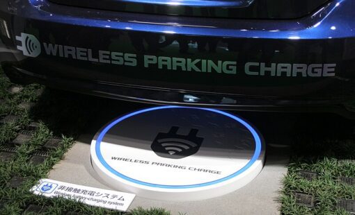
Die drahtlose Energieübertragung (Wireless Power Transfer, WPT) ersetzt Kabel und Drähte in vielen Bereichen. Die Lösungen von Zuken unterstützen Ingenieure bei der Entwicklung, Simulation und Validierung von WPT-Systemen.
- Blog
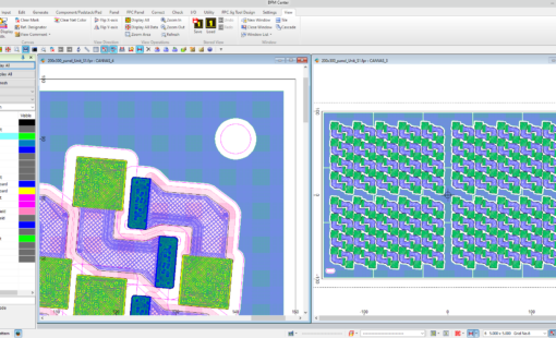
Der PCB-Markt setzt sein kontinuierliches Wachstum fort. An der Spitze dieses Wachstums steht der Sektor der Flex-PCBs. In diesem Blogpost zeigen wir Ihnen das Potenzial von Mehrfachnutzung in der Fertigung von Flex-PCB-Designs und untersuchen mögliche Kosteneinsparungen.

- Blog
Das Release 2021 von CR-8000 Design Force wartet einmal mehr mit einer Fülle von neuen und verbesserten Funktionen in der gesamten Tool-Suite auf.
Related Content
- Products
Zusätzlich zum Multi-Board PCB Design unterstützt Design Force auch die Entwicklung von IC Packages für Wire-Bond, Flip-Chip und High-Density Advanced Packaging
- Products
Design Force kombiniert konventionelles 2D-Design mit nativem 3D-Design und den neuesten Technologien in Benutzeroberfläche und Grafik für schnellstes Rendern und Aktualisieren.
- Products
CR-8000 umfasst eine Suite von Anwendungen, die den gesamten Lebenszyklus des PCB Engineerings abdecken.