MultiCore CPU support for ultra-fast simulation performance.
As data rates increase and PCB architectures grow more complex, the need for reliable signal-integrity analysis during layout also grows. Design Force SI Advance addresses this directly. The extension integrates powerful analysis capabilities into the familiar design environment and enables engineers to secure critical high-speed paths at an early stage.
The package covers the full analysis spectrum, from precise impedance determination and field-solver-based modeling through to IBIS-AMI analysis of demanding SerDes channels. This gives designers a robust foundation for well-informed decisions in routing and constraint management.
Design Force SI Advance combines a range of new functionalities to enhance your signal integrity analysis capabilities. This new, comprehensive bundle covers all aspects of Signal Integrity from Characteristic Impedance to IBIS AMI analysis of SerDes channels.
MultiCore CPU support for ultra-fast simulation performance.

64-bit computing architecture for large data records and to support parallel processing

AI/ML-assisted S-Parameter modeling
Our suite of powerful tools offers a host of benefits to ensure your electronic projects thrive, optimizing signal integrity in every step of the design process.
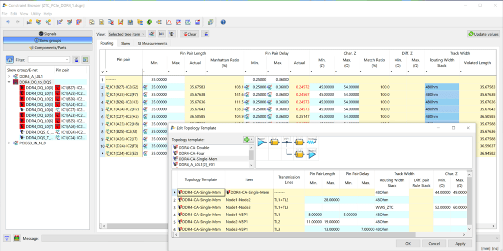
In the essential pre-layout phase, you are recommended to define the relevant high-speed constraints and to optimize the topology of critical nets (e.g.; double data rate signals). This early planning sets the stage for a robust physical design, reducing costly errors downstream and ensuring your project stays on track.
Our integrated EM field solver supports lossy interconnect models, manufacturing Tolerances, and material roughness, which empowers you to plan impedance meticulously. This approach minimizes signal loss and maximizes performance, ensuring your designs meet high standards.
Time-domain simulation provides rapid, interactive feedback on timing behavior, reflections, and crosstalk. Simulation results update quickly as design conditions change, giving clear visibility into waveform quality and delay characteristics. This responsiveness supports early identification of signal-integrity concerns and helps evaluate corrective options without disrupting the design flow.
The simulation environment supports a broad range of model types, enabling consistent access to the behavioral data required for accurate signal-integrity analysis. IBIS, SPICE, and S-parameter models can be organized and maintained within a unified library structure, ensuring that device behavior, interconnect characteristics, and frequency-dependent effects are represented with the necessary fidelity throughout the design process.
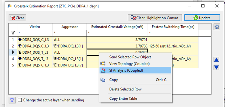
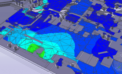
Crosstalk behavior in coupled routing can be screened quickly using field-solver results and device models in the Crosstalk Estimation report. This highlights areas where coupling may affect timing or waveform quality. When deeper insight is needed, a full crosstalk simulation quantifies aggressor–victim interactions, giving early visibility into interference and supporting signal-integrity decisions.
SPICE and S-parameter models can be used directly in the time domain, offering flexibility in how active devices and passive interconnects are represented. SPICE captures nonlinear behavior, while S-parameters describe frequency-dependent effects, allowing the simulation approach to match circuit characteristics across a wide range of scenarios.
IBIS buffer models provide a standardized way to represent I/O behavior, allowing simulations to align with industry expectations and integrate smoothly into established workflows. Their use ensures consistent switching, clamping, and timing characteristics across different devices. When Power-Aware IBIS models are included, additional effects such as simultaneous switching noise (SSN) are captured, giving a more complete view of how drivers and receivers behave under real operating conditions.
Parameter sweeps make it possible to observe how changes in geometry, spacing, or material settings influence interconnect behavior. This approach reveals the operating window for a given topology and highlights the conditions under which performance margins tighten or improve. The resulting insight supports topology choices that remain robust across expected manufacturing and environmental variations.
Time-domain simulation depends on S-parameter data expressed in the frequency domain. AI and machine-learning methods support the vector-fitting process by identifying stable parameter sets that accurately represent the modeled structure.
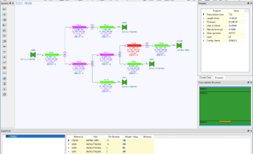
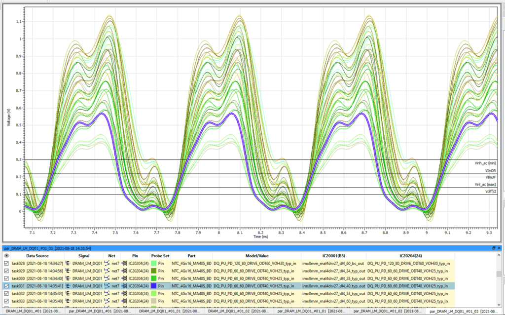
Automatic timing, skew, and signal-integrity measurements provide a clear view of waveform quality, edge behavior, and alignment between related signals under operating conditions.
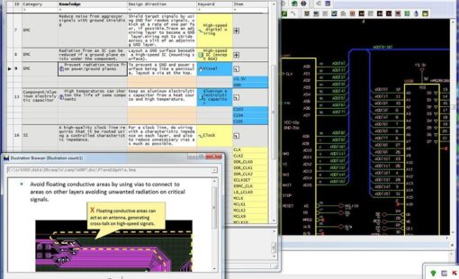
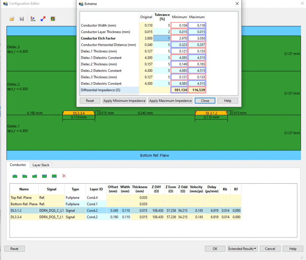
Variations in dielectric properties, copper thickness, and etching tolerances can affect impedance and propagation delay. Awareness of these effects supports more reliable stack-up and routing decisions, especially in high-speed designs where small deviations can influence performance margins.
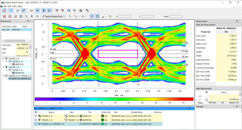
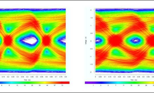
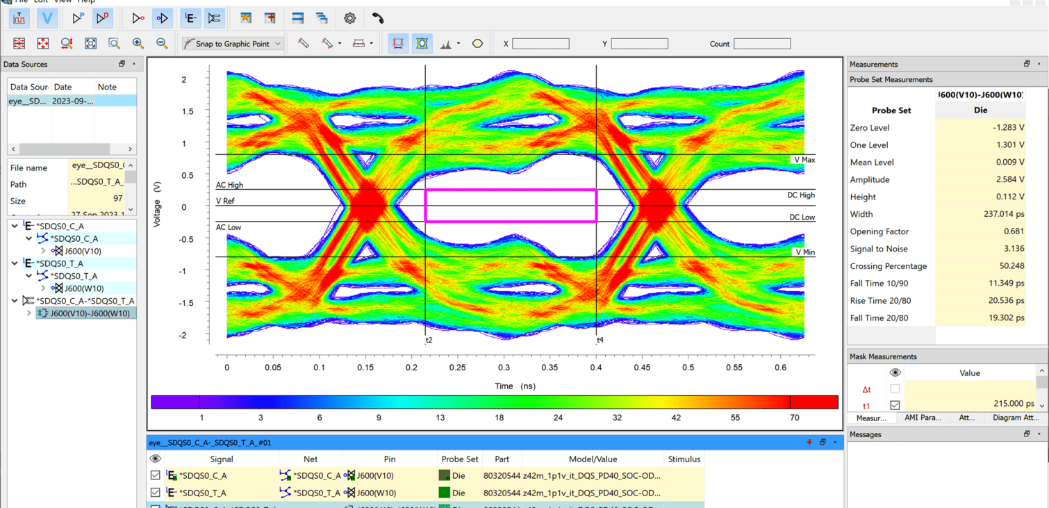
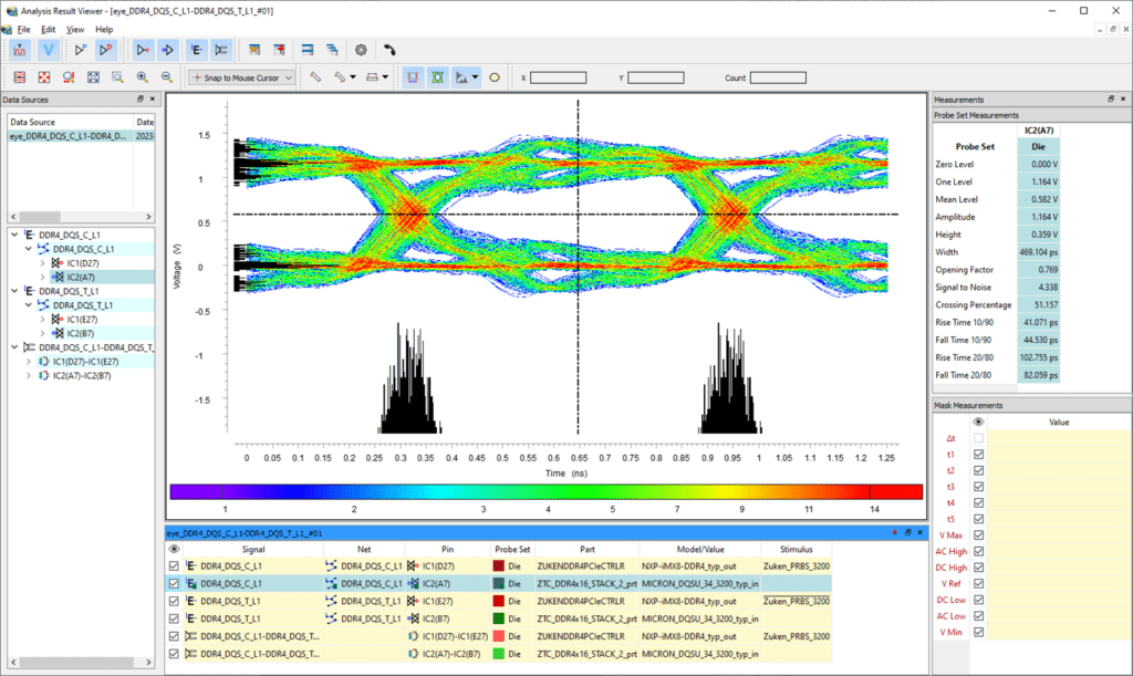
Time-domain eye analysis shows signal quality for parallel buses and serial links. Eye opening, jitter, and noise margins reveal how interconnects behave under realistic switching and indicate available performance margins.
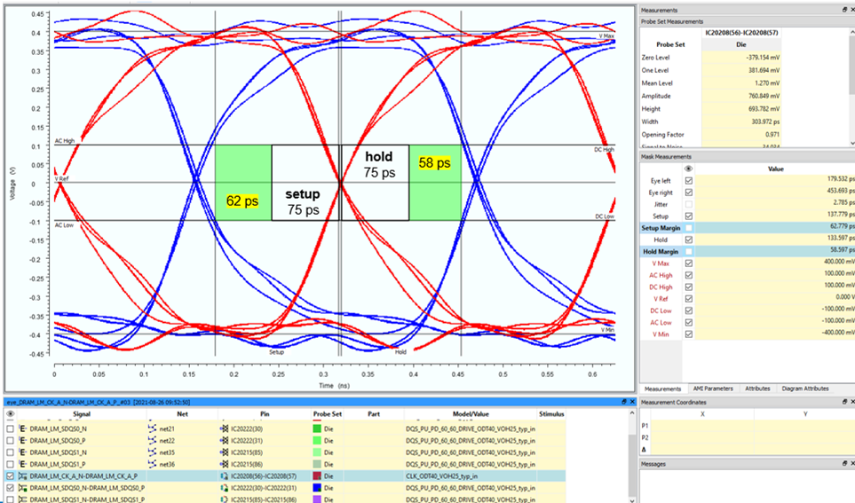
Setup and hold timing appears directly in the analysis results, showing how data and strobe signals align during operation. This view highlights margins and potential violations, supporting timing verification for high-speed interfaces.
Eye masks can be defined to represent the signal-quality requirements for a given interface. Once applied, simulation results are measured against these masks to determine whether the observed eye openings meet the specified criteria. This comparison provides a structured method for assessing compliance and highlights conditions where performance margins may be reduced.
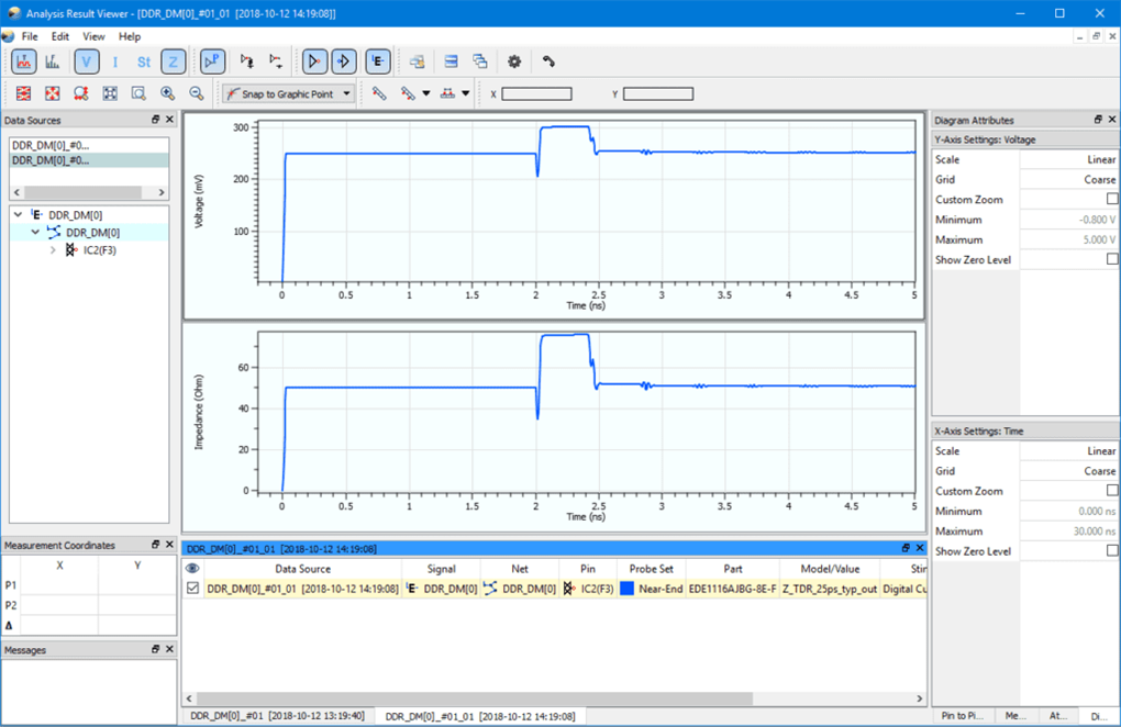
Time-domain reflectometry (TDR) provides a direct view of impedance variations along an interconnect. The resulting waveform highlights discontinuities from geometry, material, or via changes. These insights show where reflections may occur and how routing or stack-up adjustments influence signal behavior, supporting more reliable interconnect design.
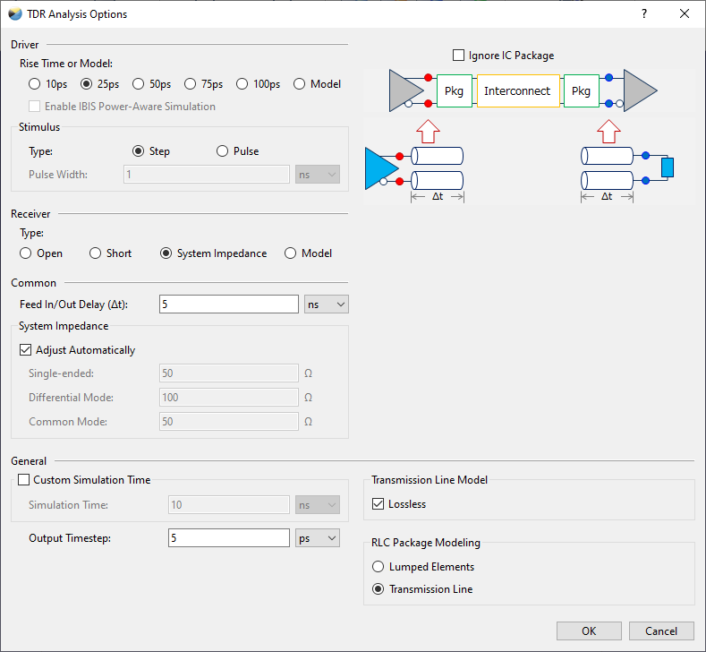
TDR results provide visibility into impedance profiles for single-ended and differential interconnects. The measurements show where mismatches arise from geometry changes, material variations, or coupling effects. Because no IBIS buffer models are required, the method supports model-less signal-integrity evaluation and enables early verification of interconnect quality.
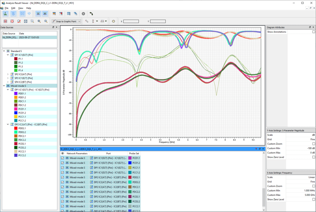
Wideband S-parameter calculations characterize interconnect behavior across frequencies up to 15 GHz. The resulting data captures frequency-dependent loss, reflections, and coupling, providing a foundation for evaluating high-speed performance and determining how routing choices or stack-up adjustments influence signal quality at gigahertz operating ranges.
Mixed-mode S-parameters extend this characterization to differential structures, separating differential- and common-mode behavior. This analysis clarifies how coupling, imbalance, or asymmetries affect performance in complex interconnect scenarios, offering a more complete picture of signal behavior for high-speed differential links.
Causality checks ensure that S-parameter data reflects physically valid system behavior. When required, causality enforcement aligns the frequency-domain response with time-domain expectations, preventing non-physical artifacts in subsequent simulations and improving the reliability of waveform and eye-diagram predictions.
S-parameter data can be exported in Touchstone format, allowing the results to be used directly in external simulation environments. This capability supports compatibility with industry-standard analysis tools and helps maintain a consistent workflow across teams and verification stages.
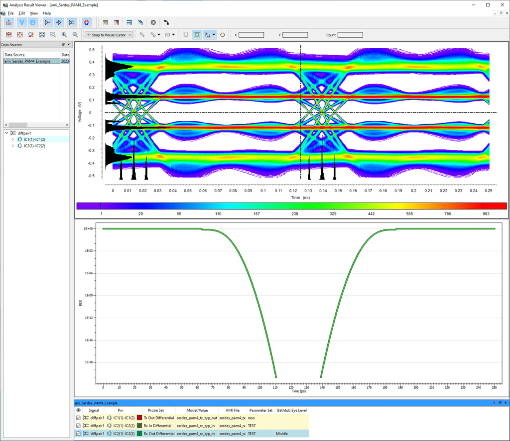
AMI-based simulation models gigabit SerDes channels under realistic conditions, capturing equalization behavior, jitter tolerance, and channel loss. The results show how transmitter and receiver settings affect eye opening and bit-error performance, supporting decisions that strengthen high-speed link robustness.
BER evaluation quantifies the likelihood of bit errors in a high-speed channel, providing a direct measure of communication reliability under expected operating conditions.
Serial links can be characterized through S-parameters, transfer functions, and impulse responses, providing a concise view of frequency- and time-domain channel behavior.
Deterministic and random jitter in both transmit and receive paths are accounted for, clarifying jitter tolerance and its impact on signal integrity.
Eye patterns and bathtub curves present signal quality and reliability metrics in a clear, interpretable form.
AMI model parameters can be adjusted through a simplified interface, supporting efficient setup and consistent simulation control.
Eye openings and signal-to-noise ratio (SNR) are measured to quantify signal quality and assess available performance margin.
Related Resources
In this Webinar, you will discover how to streamline your PCB design process with CR-8000, and seamlessly integrate prototype testing results using NoiseKen for enhanced accuracy and performance.
In this Webinar, an optimized PCB design flow combining Zuken CR-8000 technology working tightly with stackup optimization capabilities provided by Polar Speedstack ™ will be presented.
Using the example of the analysis of SerDes transmission paths such as PCI Express, SATA or USB3, we explain the methodology of an analysis- and constraint-driven assembly development with CR-8000 Design Force.
In this presentation you will be introduced to the necessary steps in constraining and validation of LPDDR4 on the basis of a real design realized in CR-8000 Design Force right first time.
CR-8000 advances system-level PCB design with significant enhancements in analog simulation, SI analysis, and intelligent layout and routing
In our webinar we will provide an introduction to the challenges of signal integrity and the underlying physical effects. This will provide the basis for practical tips to address the related challenges during PCB design.
Related Blog Posts
Double Data Rate 5 (DDR5) is the next-generation standard for random-access memory (RAM). The new specification promises to bring chips that have much higher performance than the existing DDR4 modules, as well as lower power consumption. Let us show you how you can be first to market with DDR5!
To keep a good high-speed signal quality from driver to receiver on a PCB is not an easy task for designers. One of the most challenging issues is managing the propagation delay and relative time delay mismatches. Let me take you through the process...
What IC designers do to help us route high-speed PCBs
In part 1 of this blog we took a back-to-basics approach and discussed line impedance and its effects in signal integrity. As every electrical conductor comprises capacitance, an inductance, and a frequency-dependent ohmic resistance, and with increasing frequencies, these electrical characteristics will influence and distort the signal.
Impedance and impedance control are some of the oldest and most discussed topics in PCB design. They are especially important in high-speed design related to signal integrity. In this, the first of a two-part blog, we’ll go back to the basics of impedance/impedance control and consider what influences line impedance. In part two, we’ll set about controlling it.
Tips for when routing differential pairs - You can tell when something isn’t as clear as it should be. The same questions come up time and again. You ask three experts and get three different answers. Routing differential pairs can be like that. Why? Because “it depends” - on exactly what signals those pairs are carrying and what kind of PCB you’re creating.
Topology Planning and High-Speed Architecture Definition
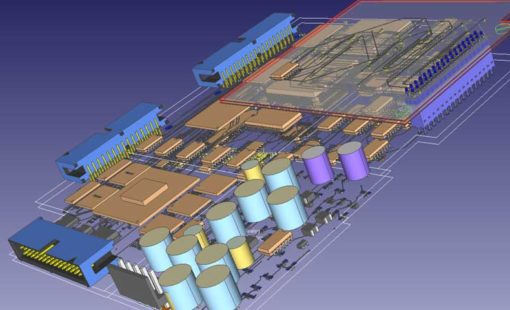
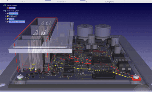
CR-8000 Design Force is the fastest, most effective PCB design solution available today. Design Force enables design teams to layout and verify their designs in the context of a complete system or product.