3D Design

- Blog
Herkömmliche CAD-Software war früher nur ein digitales Zeichenwerkzeug, das manuelle Aktualisierungen erforderte und fehleranfällig war. Da elektrische Systeme jedoch immer komplexer werden, haben intelligente CAD-Systeme den Entwurfsprozess verändert. Mehr dazu in unserem Blog.

- Blog
Seit mehr Jahrzehnten gilt 3D als der Stand der Dinge in der mechanischen Konstruktion. In der Elektronik- und Elektrotechnik hat 2D nach wie vor noch seinen festen Platz, denn hier bildet das logische Schema die Grundlage für die gesamte Konstruktion. Die dritte Dimension kommt erst bei der physikalischen Auslegung ins Spiel – dort wird sie aber immer wichtiger. Warum das so ist, lesen Sie in unserem Blog.
- Blog
Viele Jahre lang war das Layout einer Leiterplatte in 2D für die meisten Mainstream-Technologien ausreichend. Heute stehen Produktentwickler im Elektronikbereich jedoch vor neuen Herausforderungen, ausgelöst durch Megatrends wie beispielsweise das Internet of Things. Können die heutigen CAD-Tools also die neuen Anforderungen erfüllen und die Vorteile der neuen Technologien ausschöpfen?
- Blog
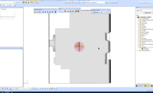
This video will show step by step instructions on how to create a basic Panel Model and insert a 3D STEP file.
- Blog
PCB design tools were built on 2D software methods in the 1980s. Many of today’s design tools still use that 2D code base. Mechanical tools have moved on to native 3D design. PCB has been stuck more or less in the 2D world. Extensions to the 2D code base made 2.5D and 3D visualization possible. But designing in 3D requires the tool to be built on a 3D kernel.
- Blog
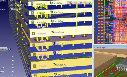
We’re happy to announce that Speedstack, Polar Instruments’ layer stackup design/documentation tools, can now be directly linked to Zuken’s CR-8000 Design Force and DFM Center.

- Blog
This video illustrates the process of creating a new terminal to be used with your connectors in Zuken’s E3.series. It covers the attribute information that can be applied to this model, and the model needed for the correct terminal for any given wire size.

- Blog
This is an exciting time in the product development world. Increasing product complexity is driving the need for a design process evolution. Not long ago the detailed design process was the centerpiece of product development. But the need for functional and physical design accuracy is forcing the product development process to evolve. In response, the product development process is both converging and expanding.
- Blog
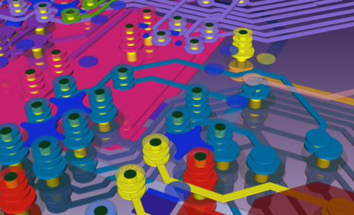
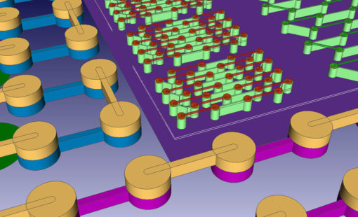
Advanced packaging techniques such as system-in-package (SiP), fan-out wafer-level packaging (FOWLP), 3D die stacks, etc. have been around for over a decade, yet with any other EDA design tool, it is still a tedious, time consuming, and error-prone process to implement these designs.
- Blog
During PCB West Exhibition Day, Sierra Circuits met Humair Mandavia, Chief Strategy Officer at Zuken. After his joint interview with Simon Fried, CBO of Nano Dimension, we discussed 3D PCB designing, and Zuken’s product, CR-8000 with him.

- Blog
Sierra met Steve Watt, Manager of PCB Engineering at Zuken, during PCB West 2017 at the Santa Clara Convention Center. After his presentation on how to improve flexible printed circuit manufacturing, he shared a few tips in front of our camera. Listen to him discuss CR-8000, DfM checks, and flexible PCB designing.
- Blog
It’s 25 years since the first FED Conference took place in Berlin back in 1993, as a gathering for the German-speaking electronic and PCB-related industry. This also happened to be the year we consider as the birth of high-speed design.

- Blog
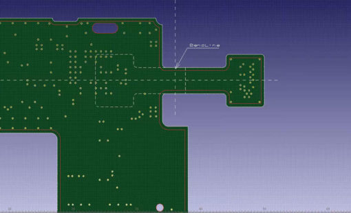
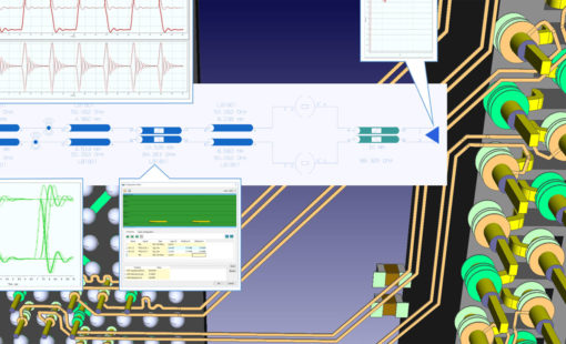
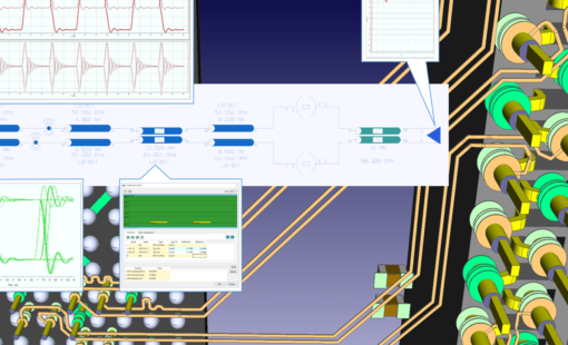
The PCB design team at Renishaw work with flex PCBs and flexi-rigid boards that require detailed signal integrity analysis. To achieve the most accurate results they are working with Zuken’s electronic PCB design software to visualize boards in 3D using imported MCAD data. This also ensures that sure high-speed digital signals can be transmitted with minimal distortion.
- Blog
Ultra-high signal speeds demand detailed consideration of the third dimension in PCB design, including via structures and layer stacks. Today I’m going to focus on the challenge. In my two subsequent posts I’ll be reviewing what PCB designers can do to meet that challenge.