The High-Speed Design Challenge of Maintaining PCB Signal Integrity in a 3D Design Environment
Ultra-high signal speeds demand detailed consideration of the third dimension in PCB design, including via structures and layer stacks. Today I’m going to focus on the challenge. In my two subsequent posts, I’ll be reviewing what PCB designers can do to meet that challenge.
Mainstream High-Speed Signals
Not long ago, third dimension issues didn’t figure too much in high-speed design calculations; but signals have become so fast that those vias don’t affect them the same way they did before. Those really fast signals have become part of super-common bus standards that are used in all kinds of products.
It’s a PCB design issue that we can’t avoid. Luckily, there are ways not just to address this issue, but to optimize performance at the same time.
Effects of Vias on PCB Signal Integrity in High-Speed Designs
Layer changes can slow signals down or distort them. Their effects depend (amongst other things) on:
- Via geometry
- Where vias are placed within the routing
- Shape and speed of signals
- Other nearby items that couple to vias
So vias don’t always distort signals in the same way and neither does the same via always introduce the same delay.
New Via Technology Threshold
A key breakpoint is reached when a signal is so fast that the routing that carries it starts to behave as a network of transmission lines. When this happens, engineers must take positive steps to make sure signals arrive in good shape.
For mainstream digital designs, that breakpoint was reached decades ago for routing in the XY plane. That’s why we’ve long had controlled routing topology and reference ground and power planes. But now we’ve reached the point where we need to do the same in the third dimension. Standards-based bussing means that this can happen even on a board that doesn’t run particularly quickly.
If you’d like to see me describe all that with the help of a sheet of hardboard, you can watch this short movie.
See you again in Part 2 where I look more at how to use vias to maintain PCB signal integrity under these high-speed 3D conditions.

-
Electronic Design Technology Partner

- Blog
Modern electronic products are no longer built around a single PCB. As systems become faster, denser, and more interconnected, engineering teams are being forced to rethink how they design, verify, and manage complex multi-board products.
- Blog
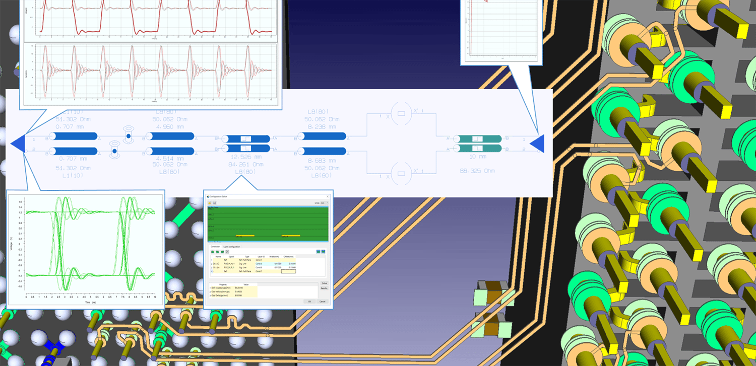
Explore how CR-8000 enhances PCB design with integrated control of impedance and resistance—enabling precise analysis for both high-speed and high-power applications, from signal integrity to power distribution optimization.
- Blog
High-Speed-Serial-Links wirken oft wie schwarze Magie – steigende Datenraten verstärken dieses Gefühl. Donald Telian (SI Guys) und Ralf Brüning holen die Diskussion zurück zu den Grundlagen.
- Blog
Lerne die beiden wichtigsten Grundlagen für den zuverlässigen Entwurf von High Speed Serial Links und erfahre, wie du Herausforderungen bei der Signalintegrität bei Geschwindigkeiten von mehreren Gbit/s meistern kannst.