
PCB Design Data Management: Expectation vs Reality

From our everyday life, we know many examples where our expectations and reality do not quite match. PCB design data management is no exception.
During product development, CAD designs are constantly in flux. Engineers from different departments work together on a product design, customers adjust their requirements, suppliers change their products and specifications, and manufacturing demands simplifications. In the process, many different stakeholders access data at the same time, while designs continue to evolve. This results in different file formats that need to be linked together to comprehensively model a product.
The Expectation
The dream of many IT managers is one central software solution that manages all of a product’s data. The advantages of such a solution with a “single source of truth” (SSOT) are obvious. Duplicate data entries are eliminated, up-to-date data is available at the right time, and the time spent searching for information is reduced to a minimum. In short: all parties involved use the same data to make decisions and are ideally at the same level of knowledge.
Companies can thus react more quickly to market dynamics and better implement product innovations. In addition, such a solution only requires a few interfaces. This avoids complicated interface management and data clutter from intermediate storage.
The Reality
However, the reality is for the most part still far off from these expectations. PLM systems simply cannot manage native CAD data. They store such data as zip containers. So, anyone who wants to access and edit complete data sets must do so in their native systems. That is why the number of different ERP, PLM, and design systems connected by numerous interfaces is growing. This is not due to a lack of interest or motivation for optimization, but rather because the described ideal is hardly feasible.
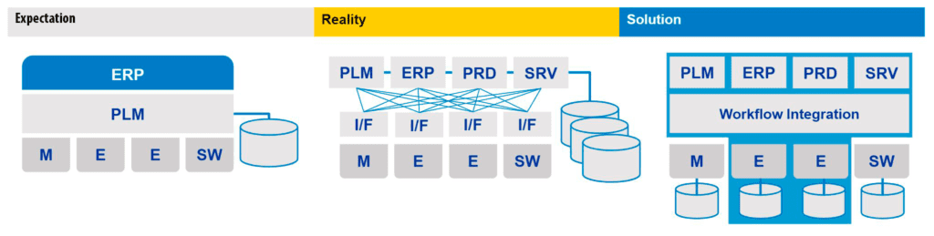
For this reason, Zuken offers a workflow integration with the aim to reduce the number of necessary interfaces while still enabling native data management with a single source of truth. This integration consists of the EDM system DS-CR, which can connect to all higher-level PLM/ERP systems (SAP, Teamcenter, Windchill, Aras Innovator, DS Enovia, etc.). Through this connection, data is exchanged in both directions. For example metadata for article management, parts lists, circuit diagrams as PDF or Gerber files.
PCB Design Data Management with the Engineering Desktop
DS-CR is designed to support the specific requirements of PCB design data management. The so-called Engineering Desktop (EDT) is where all of the design data management takes place. All PCB design data is safely stored in a “Vault”. Engineers can download designs from the project PCB library to a local computer via a check-out for editing on the go.
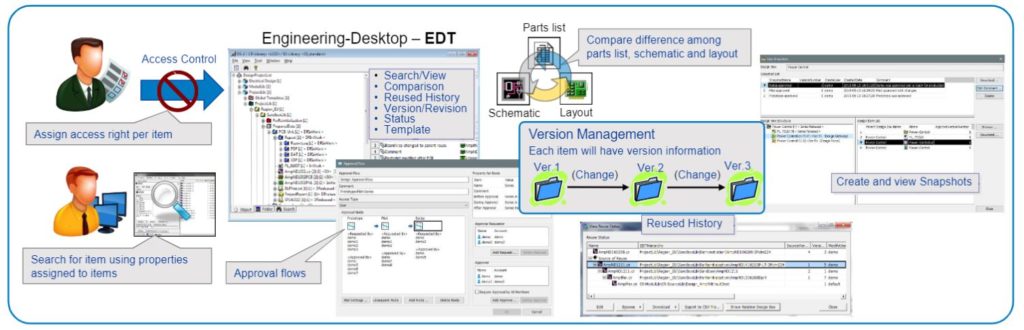
The automatic versioning at each check-out and check-in replaces error-prone manual versioning and provides a project history including all revisions. Each of these versions can serve as a starting point for a new PCB design via the reuse function.
The Vault is protected by role and configuration management, where specific access rights can be assigned to any user. In addition, all objects can be issued with an approval flow. Should there be a pad or padstack which has been further engineered and consequently can no longer be used in production, it is locked by a status change. In this way, an obsolete component can no longer be used in the workflow.
Component Management with the Component Master
With the Component Master, metadata (price, MTBF value, ROHS determination, etc.) can be retrieved from the PLM/ERP system in addition to footprint, pad, and padstack. Usually, there is a datasheet, a test result, a specification, and the designer always has to carefully watch which data pots he is using to build the documentation or components. DS-CR manages all this in a single source of truth, in which components can also be fully built using third-party tools such as SiliconExpert.
The accessible metadata also includes information on the availability of components. If one component was discontinued, alternatives can easily be found. In a nutshell: The Component Master contains all important information and can also be controlled from the CR-8000 PCB design environment.
With these extensive PCB data management capabilities, DS-CR combines a true single source of truth with native data management for the development of PCBs and other electronic systems.
Learn more about DS-2 – engineering design data management software.
Learn more about DS-CR – PCB library and design management for CR-8000.
The key features of DS-CR summarized:
- Single source of truth for the development of electronic systems
- Automatic versioning and complete project history
- Design reuse possible from any point in the product development process
- Great depth of information from meta-data
- Ability to define approval flows.
You can find all details about PCB design data management with DS-CR explained in a practice-oriented way in our webinar. Watch it now or on-demand later.

- Blog
EREMS, a French enterprise specializing in the design and realization of high-tech electronic equipment and of associated software for Space, Defense, and Aeronautics uses CR-8000 and DS-CR from Zuken for the design and lifecycle management of flight electronics, ground electronic equipment, and test benches.

- Blog
Today's smart and connected products require the interaction of different components and systems. Their elements are developed in different engineering disciplines and departments. These disciplines speak different engineering languages and require unique views of the same product. The storage of these different versions in the respective departments leads to disconnected silos in terms of processes and data - but digital continuity is here to help!

- Blog
Have you ever tried to remember what changed between revisions of a design and then had to do a painstaking review of the two designs? With the comparison functions in DS-CR, even the smallest changes or unintentional deviations between different revisions of a PCB design can be quickly identified.

- Blog
The world that we all live in has been changed by the Covid-19 outbreak. Stay at home orders and social distancing significantly impact the way we live our daily lives. Working remotely presents a whole new set of challenges for engineers and the companies that employ us. We now work on company supplied-laptops that typically connect back to the corporate network through a VPN.