EMC Compliant PCB Design: Identify EMC Problems
Menu
Electromagnetic interference (EMI) is inherent in every electronic device we use today. Cell phones or IoT applications, such as fitness trackers or smartwatches, come in ever shorter innovation cycles. To keep up with innovation, time-consuming re-design cycles should be avoided under all circumstances. Problems with electromagnetic compatibility (EMC) in PCB design are often responsible for said re-design cycles. While it is impossible to completely eliminate EMI/EMC, we can make our PCB design less vulnerable to EMI/EMC effects.
What is EMC in a PCB?
Electromagnetic compatibility (EMC) is the branch of electrical engineering and physics that deals with the unintentional generation, propagation, and reception of electromagnetic waves (in the E and H fields). These can subsequently lead to functional interferences, malfunctions, or even physical damage in electronic devices.
Generally speaking, to achieve an EMC compliant design, PCB designers have to consider three basic aspects:
- The emission referring to the unwanted generation of electromagnetic radiation by a source and its propagation to the sinks.
- The respective vulnerability to electromagnetic interference electronic systems or components.
- An electronic system should, most importantly, not cause intolerable electromagnetic interference with itself.
To say it in a simple way, EMC is the ability of electronic systems to function in a common electromagnetic environment without, first of all, being affected by other systems, second of all, interfering with other systems, and finally, interfering with itself.
Know the Potential EMI Sources
On a printed circuit board, there are various potential sources of interference, that can cause a variety of potential effects from the following categories:
- Conducted emission (signal and power integrity)
- Radiated emission
- Immunity to radiated and conducted emissions
- ESD
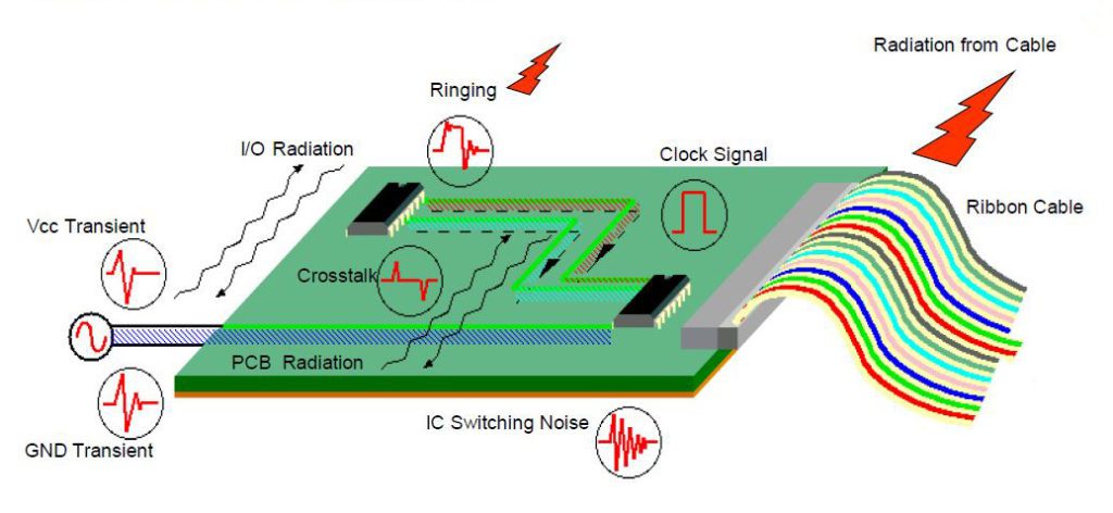
Conducted emission passes through power input lines and cables into an electronic system. Radiated emission on the other hand is created by electromagnetic waves from power and communications lines, electrostatic discharges, and switching devices.
Often unnoticed by PCB designers, the ribbon cable on a PCB connector, for example, physically forms the arm of a dipole and thus forms a parasitic antenna. In this case, current and voltage peaks occurring during the switching process of the active components in the power supply can lead to an excitation of this parasitic antenna. This would result in an increased radiation pattern.
In addition, the signal shapes in digital signaling are, in theory, ideal rectangles. Nevertheless, in reality, they don’t exist in such a form. Instead, the signals are more or less distorted and disturbed. The resulting voltage peaks of the reflections and crosstalk will also have a negative effect on the EMC behavior.
Integrating EMC Compliant PCB Design into Product Development
EMC compliant PCB design is crucial to the success of a product. Only by complying with the EMC regulations of the specific target market or application can products get approved for customer deployment. However, designers often only discover issues during prototype testing. Besides a lack of know-how is often due to a lack of integrating proper EMC verification procedures into the design process.
To manage EMC in the design process and to detect problems at an early stage there are several options. The first step should be the systematic definition and use of design constraint processes, especially for signal and power integrity issues.
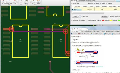
Tool-supported EMC Design Reviews
Tool-supported EMC design reviews can ensure that PCB designers follow the relevant EMC guidelines. CR-8000 Design Force comes with EMC Design Rule Checks, where specific rules can be selected or deselected as well as prioritized on a per-user or per-design base. The circuit designer can classify EMC-relevant signals for such checks as early as in the schematic design. The EMC rules suitable for an application are then selected and applied during the design phase.
The direct integration into the CAD process (2D and 3D) and the automatic generation of reports in the form of DRC checks which are familiar to any layout engineer, simplify the workflow. The development team can share these reports with images, respective progress status, and approval information as Excel documents. The design data stores this information for joint forces on EMC aspects in the design team.
The rules implemented in the EMC-Adviser for Design Force contain recommendations for various design issues that enable non-experts to solve signal integrity, power integrity, and electromagnetic compatibility problems and thus help to develop an error-free, EMC-compliant layout. No additional software is required to validate the identified potential EMC issues.
My “First-Aid-Kit” for EMC compliant PCB design
For an EMC compliant PCB design, it is essential to consider (at least, but of course there are many more) the following four aspects:
1. Identify and evaluate parasitic antennas
It is essential to work out where parasitic antennas could form on the PCB. Parasitic antennas are developing electrical or magnetic monopole or dipole structures.
Shielding, a mechanical technique, uses conductive/magnetic (or both) materials to prevent radiation from parasitic antennas. A conductive container connected to the ground effectively reduces the loop antenna size by reflecting and absorbing part of its radiation. EMI/EMC shielding protects the signal transmission from external interference and prevents information loss.
2. Recognize and account for the current return paths
An electric current inevitably returns to its source. According to Faraday’s law, what makes the difference is how the signal runs through the system. Thus, visualizing the return paths and the return loops plays an important role.
Depending on the application, the returning current either runs along the path with the lowest impedance or the path with the lowest resistance. Longer paths create a ground loop, which forms a radiating antenna and leads to crosstalk. A short return path has the advantage of lower impedance and therefore resulting in better EMC. Designers should keep the return paths as short and the loop area as small as possible and where possible they should not wire lines across slots, not even in differential pairs.
3. Understanding the various coupling effects
Coupling paths between the source and the sinks can occur either through parasitic voltages or currents or relate to IO. In many cases, their roots are often not immediately recognizable in the layout.
ICs, in operation, switch current at a high frequency, resulting in switching noise in the connected power rails. If not controlled, this noise will result in radiated emissions and thus EMI. The methods to reduce noise on the power lines are to place the decoupling capacitors near the IC power supply pins or grounding capacitors directly to the ground planes. Using power supply planes instead of power supply lines will also reduce power noise.
Impedance matching between source and sink is critical when a circuit is operating at high speed. Signal reflections and high-frequency ringing will occur unless the impedance is properly matched and controlled. Excess RF energy radiates to other parts of the circuit and causes EMI problems. Signal termination strategies help reduce this and can also slow the fast-rising and falling edges of signals. The trace impedance depends also on the materials used on the PCB.
4. Understanding resonances as potential antennas
Almost all electrical structures can become resonant. This includes single lines and differential signals, and also power supply structures, cables, packages, even vias. Fortunately, the resonance frequency for many structures can be easily calculated using this formula: fres=1/(2π√L∙C).
However, knowledge of the values for the (parasitic) inductances (L) and capacitances (C) is not quite so easy to obtain and often requires complex analysis. Also, resonances cannot be completely erased. It is important to know and understand the effect and to avoid excitation – where possible.
You can find these and other tips for EMC compliant PCB design explained in detail and practice-oriented in our webinar

Ralf works as Product Manager for High-speed Design Systems at the Zuken EMC Technology Center in Paderborn/Germany, responsible for product marketing and business development for the Zuken SI, PI and EMC analysis tools. He holds a diploma degree in computer science, electrical engineering and economics from the University of Paderborn. He has 30 years of experience in Electronics and EDA. He is regular speaker on international conferences, but is involved in European Funding project and standardization activities as well.

- Blog
May 23, 2025
AI in PCB Design: From Misconception to Meaningful Assistance
AI in PCB design is increasingly seen as a game-changer, with some predicting it could soon replace entire layout teams—but this view risks overlooking both the current limits of AI and the critical expertise engineering demands. At DesignCon 2025, experts from emphasized that AI's real value lies in complementing human judgment, not replacing it. Read more on our blog.
Read now

- Blog
February 13, 2025
The Future of Augmented Reality
Our new post explores the potential of augmented reality (AR) to transform everyday experiences in shopping, education, and navigation. It highlights how enhanced AR devices will offer immersive, interactive environments that blend the virtual and physical worlds.
Read now

- Blog
January 30, 2025
The Top PCB Design Trends to Watch in 2025
The field of PCB design continues to evolve as advancements in technology and shifting market demands push the boundaries of what’s possible. By 2025, several key trends are set to shape the industry. Find out more on our blog.
Read now

- Blog
January 23, 2025
Supply Chain Risk Management in PCB Design with SiliconExpert and CR-8000 Integration
Supply chain risk management is critical for electronics design. By integrating SiliconExpert with CR-8000, engineers gain tools to streamline component selection, manage obsolescence, and ensure design continuity. This integration supports efficient workflows, reduces costs, and mitigates supply chain disruptions.
Read now