Building Confidence in SERDES and DDR Performance Before Prototyping
Menu
A SERDES interface like PCI-Express Gen5 and higher can satisfy its routing constraints and still produce intermittent link errors during system validation. A modern DDR interface can meet its length- (in fact delay-) matching rules and still show timing failures when the prototype is tested under real operating conditions. For PCB designers, these are among the most frustrating problems in high-speed design.
The layout appears correct. Impedance targets have been followed. Differential pairs are matched. DDR byte lanes satisfy their routing constraints. ECAD-Design rule checks all pass.
Yet the problems only emerge later, when the complete hardware is assembled and operating at speed.
The reason is straightforward: SERDES and DDR performance depends on more than whether individual PCB routing rules have been satisfied. What ultimately matters is the electrical and timing behavior of the implemented channel.
As interface speeds increase and design margins become tighter, small effects from vias, connectors, stackups, return paths and return-path-discontinuities (RPDs), crosstalk and accumulated skew can determine whether a design operates reliably or fails during validation.
Why Do High-Speed Designs Pass Layout Checks but Fail in Hardware?
PCB constraints are essential because they translate electrical requirements into physical design rules. They control parameters such as impedance, spacing, topology, maximum length and skew.
But constraints describe what the layout should achieve. They do not always prove how the finished interconnect will behave electrically.
A trace may meet its target impedance while vias introduce discontinuities. Two signals may satisfy a length-matching rule while propagation delay differs because they travel through different structures. A PCIe differential pair may be routed correctly on one PCB but experience additional loss when a connector, cable or second board is included in the complete channel. This distinction becomes increasingly important as signal margins shrink.
The challenge is therefore not simply to route a SERDES link or a DDR interface correctly. It is to verify that the implemented design still satisfies the electrical requirements that motivated those routing rules in the first place.
SERDES and DDR Create Different Verification Challenges
SERDES and DDR are both high-speed interfaces, but they should not be treated as the same kind of signal-integrity problem.
As SERDES signals typically implement I/O connection and are often electrally rather long, the primary concern here is whether the complete channel provides sufficient signal quality and margin at the receiver. Loss, reflections, jitter, discontinuities and crosstalk accumulate throughout the channel and influence the resulting eye opening.
DDR implements the interface to data storage device and comprising lots of signals presents a different challenge. It is a parallel memory interface in which multiple data, strobe, address and control signals are organized in groups (ByteLanes) which must arrive within tightly controlled timing relationship. Routing topology, skew and setup-and-hold margin therefore become central concerns.
The engineering disciplines overlap, but the failure modes are different. Understanding that difference is important because simply applying a generic set of “high-speed routing rules” does not provide adequate verification for either interface.
Why SERDES Problems Often Appear Late
A SERDES channel may extend far beyond a pair of traces on a single PCB. The signal can pass through packages, vias, connectors, cables, mezzanine boards or additional PCBs before reaching the receiver. Every transition changes the electrical environment seen by the signal.
Individually, these effects may appear relatively small. Together they contribute to insertion loss, reflections, jitter and reduced eye opening. That is why a differential pair that looks perfectly acceptable in the PCB layout can behave very differently in the complete product.
At lower data rates, a design may have enough margin to tolerate small imperfections. As data rates increase, the available margin becomes less forgiving. Via structures, connector models, reference-plane changes and routing discontinuities that previously caused little concern can become significant contributors to channel degradation.
The important question is therefore not simply: “Is the PCIe (or USB or any other SERDES link) differential pair routed correctly?”
It is: “Does the complete PCIe channel still provide sufficient operating margin?”
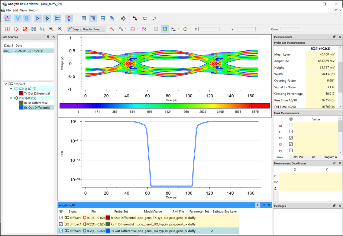
Eye-pattern analysis is particularly valuable here because it brings the accumulated effects of the channel into a single representation of timing and voltage margin.
DDR Is Fundamentally a Timing Problem pretending to be a Trace-Length-Adjustment Problem
DDR design creates a different kind of challenge.
The receiver must capture data within defined timing windows, which makes the relationship between the signals extremely important. Data signals must arrive in the correct relationship to the associated strobe, while address and command groups must remain within their specified timing budgets.
This is why length matching is such a visible part of DDR PCB design. But physical length is only a proxy for what engineers dominantly must care about: propagation delay and timing margins.
Two traces can have similar physical lengths but different electrical delays depending on stackup, layer transitions, via structures and other characteristics of the route. At the same time, routing changes made elsewhere in the design can gradually consume the timing margin originally established during planning.
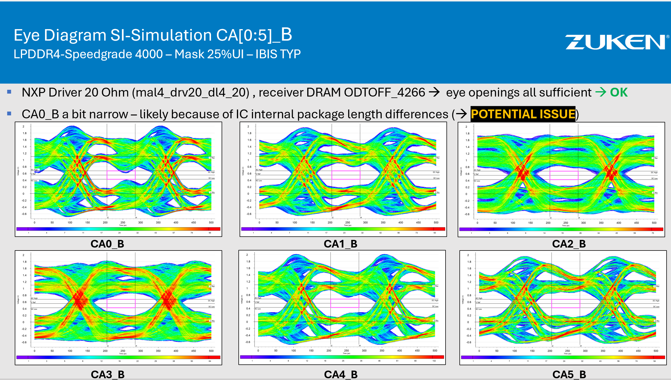
The layout may therefore satisfy a nominal length rule without proving that the full DDR interface still meets its required setup-and-hold relationships. Chip internal length differences within the memory controller for the DRAM interface ball-to-DIE connections which must be compensated on the board to match the skew rules add further fuel to the complexity fire.
This is one reason DDR problems can remain hidden until memory testing begins on physical hardware.
Small Changes May Consume Large Amounts of Margin
Late-stage failures are rarely caused by one spectacular design error. More often, margin disappears gradually.
A connector changes. A component is moved to solve a mechanical issue. A differential pair requires additional vias. A DDR route is moved to another layer. A neighboring high-speed net introduces more coupling than expected. A return path is interrupted by a plane transition.
Each decision may be reasonable when viewed individually. But high-speed interfaces respond to the combined effect of all these decisions.
By the time the design reaches prototype testing, the cumulative impact may be enough to create intermittent failures, reduced timing margin or signal-quality problems that were not obvious during PCB layout.
This is why high-speed verification needs to follow the design as it evolves rather than being treated as a final signoff check.
Constraints Need to Remain Connected to Design Intent
Another source of late problems is the gap between electrical requirements and their physical implementation.
High-speed interfaces usually begin with a set of design intentions: impedance targets, routing topologies, maximum delays, skew relationships and timing requirements.
Those requirements must survive numerous design changes before the PCB is released.
When constraints are transferred manually between schematic, planning, layout and analysis activities, inconsistencies can develop easily. A requirement may be interpreted differently, updated in one environment but not another or reduced to a physical rule that no longer reflects the original electrical objective.
For SERDES and DDR designs, maintaining the connection between design intent, constraints and verification is therefore just as important as the individual routing rules themselves.
Earlier Verification Changes the Development Process
The alternative is not to add another sign-off step at the end of PCB design. It is to move verification closer to the engineering decisions that affect performance.
For SERDES, this means evaluating signal quality while channel symetry (e.g.; differential vias with stitching via pairs), differential routing, fan-out of connectors, BGAs and via structures can still be changed. Eye-pattern and channel analysis can reveal whether the implemented path retains sufficient operating margin before a prototype is built.
For DDR, earlier verification means looking beyond simple trace lengths and examining skew, delay and setup-and-hold relationships while routing is still evolving.
This creates a much shorter feedback loop.
Instead of discovering a problem during system validation and tracing it back through weeks or months of design decisions, engineers can investigate the electrical consequences of those decisions while they are being made.
This is the practical value of left-shift of the verification in high-speed PCB design.
In a Nutshell – How to Verify SERDES and DDR Designs with CR-8000
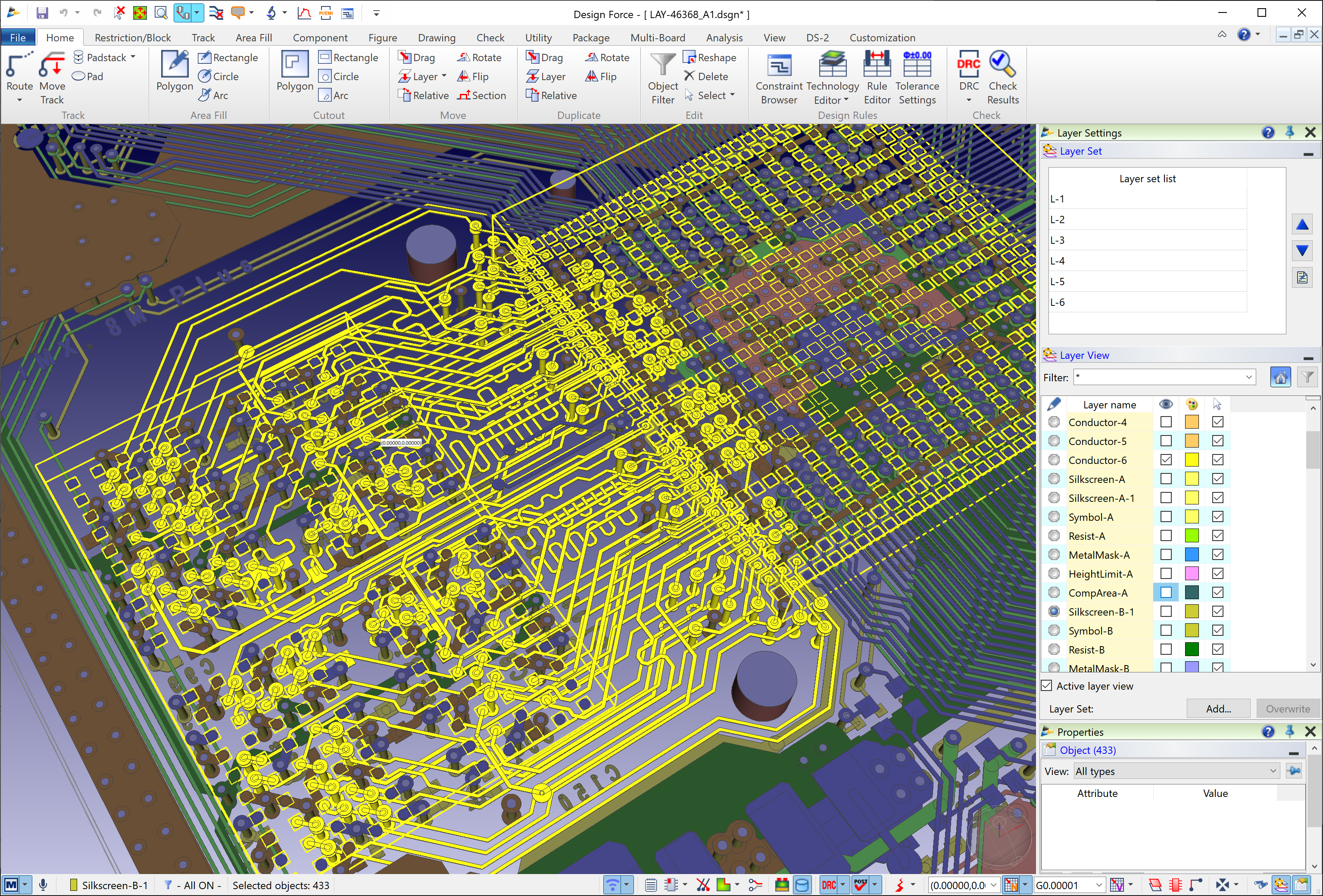
CR-8000 supports this approach by keeping high-speed constraints and signal-integrity analysis closer to the PCB design workflow.
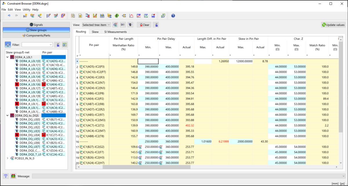
For DDR and other timing-sensitive interfaces, engineers can define and manage impedance, delay and skew relationships as well as critical-net topology. Maintaining these constraints through the design process helps preserve the electrical intent behind the physical layout.
For SERDES and other high-speed channels, CR-8000 Design Force SI Advance provides signal-integrity analysis within the PCB design environment. Time-domain eye-pattern analysis can be used to evaluate serial links, while eye masks provide defined criteria for assessing channel quality.
The same analysis environment can also provide visibility into setup-and-hold timing for parallel interfaces. TDR/TDT, crosstalk and frequency-domain analysis can then help engineers investigate the physical mechanisms behind reduced signal margin.
The objective is not simply to add more simulation, it is to connect verification with the design decisions that determine whether the interface will ultimately succeed.
From Rule Compliance to Performance Confidence
SERDES and DDR designs do not usually fail late because engineers forgot that high-speed interfaces require careful routing.
They fail late because the complete electrical behavior of the implemented system was not visible early enough.
Design rules remain essential. Length matching remains essential. Impedance control remains essential.
But none of them, on their own, guarantee sufficient operating margin.
For SERDES, engineers need confidence that the complete channel maintains adequate signal quality. For DDR, they need confidence that data, strobes and associated signals maintain the required timing relationships.
That requires moving beyond the question: “Did the layout pass?”toward a more meaningful one: “Will the implemented interface perform reliably when the product operates at the intended speed?”
The earlier engineering teams can answer that question, the less likely they are to discover the answer for the first time in the validation lab.

Ralf works as Product Manager for High-speed Design Systems at the Zuken EMC Technology Center in Paderborn/Germany, responsible for product marketing and business development for the Zuken SI, PI and EMC analysis tools. He holds a diploma degree in computer science, electrical engineering and economics from the University of Paderborn. He has 30 years of experience in Electronics and EDA. He is regular speaker on international conferences, but is involved in European Funding project and standardization activities as well.

- Blog
August 03, 2026
Understanding Eye Pattern Analysis for PCB Designers
Learn how eye pattern analysis helps PCB designers evaluate signal integrity, timing margin and high-speed communication channels. Discover how CR-8000 supports earlier signal integrity verification and eye diagram analysis.
Read now
- Blog
July 24, 2026
The PCB Passed Every Review. So Why Did the Product Fail?
PCB Design, Electronic, Blog
- Blog
May 13, 2026
Why PCB Design Has Outgrown Single-Board Thinking
Modern electronic products are no longer built around a single PCB. As systems become faster, denser, and more interconnected, engineering teams are being forced to rethink how they design, verify, and manage complex multi-board products.
Read now
- Blog
March 25, 2026
Determining Conductor DC-Resistance in CR-8000 Design Force
Explore how CR-8000 enhances PCB design with integrated control of impedance and resistance—enabling precise analysis for both high-speed and high-power applications, from signal integrity to power distribution optimization.
Read now
Related Content
- Webinar
April 12, 2024
Dealing with Component Obsolescence in PCB Design
This webinar will demonstrate how Zuken's CR-8000 Enterprise PCB Design System automates updates and redesigns in response to component obsolescence. Learn how to identify affected modules, update designs with a schematic module library, and intelligently assist layout modifications.
Watch On-Demand

- Webinar
December 04, 2023
AI-Based PCB Place and Route
CR-8000 Webinar: Zuken recently announced the upcoming release of the industry’s first AI-based PCB place and route product - Autonomous Intelligent Place and Route (AIPR) - This webinar will examine how companies and users will benefit.
Watch Now
- Webinar
July 06, 2020
Practical Signal Integrity for improved EMI Control in PCB Design
In our webinar we will provide an introduction to the challenges of signal integrity and the underlying physical effects. This will provide the basis for practical tips to address the related challenges during PCB design.
WATCH NOW

- Products
September 26, 2018
CR-8000
CR-8000 is a System-Level PCB & IC Package Design software including 3D Multi-board, Analysis and MCAD Integration
Read now
Advanced multi-board PCB design software