
Understanding Eye Pattern Analysis for PCB Designers
Menu
A high-speed interface passes simulation. The PCB is manufactured. Initial bring-up succeeds. Yet during system validation, intermittent communication errors begin to appear.
The layout meets impedance targets. Differential pairs are length matched. Design rules pass. Manufacturing files are released.
So why does communication still fail?
The answer often lies not in any individual trace or routing decision, but in the behavior of the complete communication channel. As data rates continue to increase, even small amounts of loss, jitter, crosstalk, and reflection can reduce the timing and voltage margins needed for reliable operation.
This is where eye pattern analysis becomes an essential part of modern PCB design.
Rather than asking whether a signal reaches its destination, eye pattern analysis answers a far more valuable engineering question: Does the complete communication channel provide enough margin for reliable data transmission?
What Is Eye Pattern Analysis?
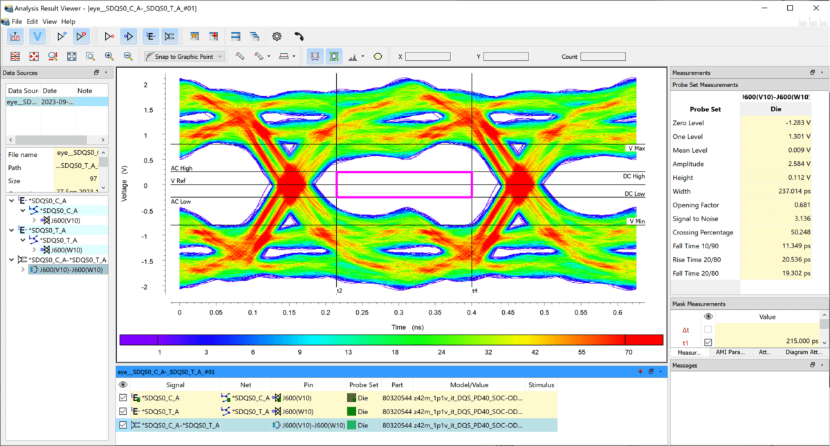
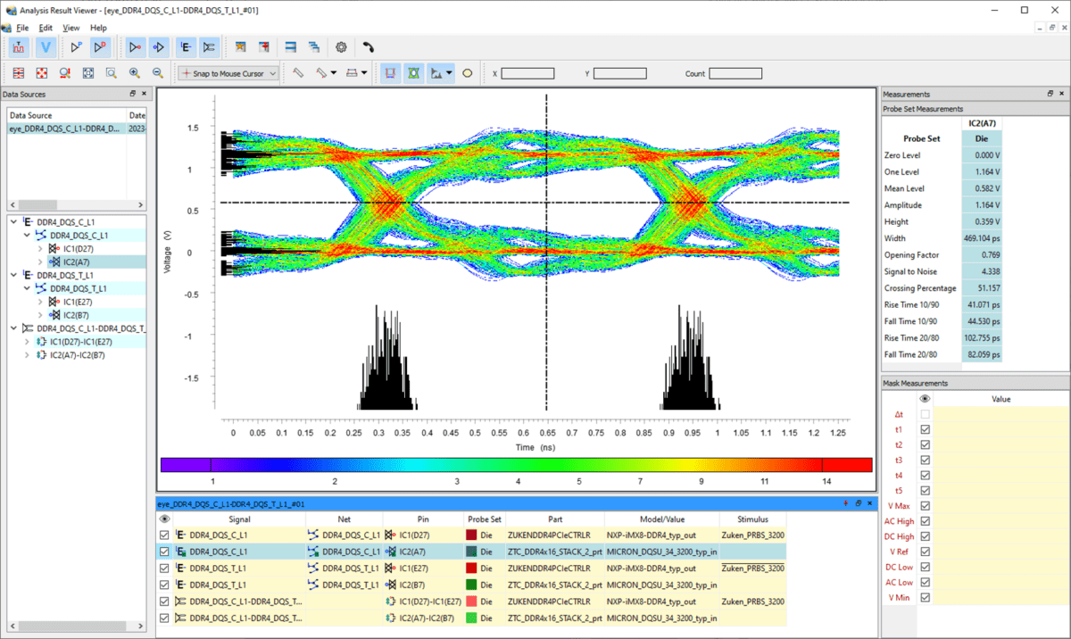
An eye pattern, often referred to as an eye diagram, is created by overlaying thousands of consecutive bits of a high-speed digital signal on top of one another.
Instead of displaying individual transitions, the resulting diagram visualizes the overall quality of the communication channel. The characteristic eye shape represents the voltage and timing margin available at the receiver, allowing engineers to evaluate whether data can be sampled reliably.
A wide, open eye generally indicates a robust channel with sufficient operating margin. As electrical effects begin to degrade the signal, the eye gradually closes. Eventually, the receiver may no longer be able to distinguish reliably between logical ones and zeros, increasing the likelihood of communication errors.
Unlike many individual signal integrity measurements, an eye diagram combines the cumulative effects of the entire channel into a single visualization, making it one of the most effective ways to evaluate high-speed digital performance.
Why Eye Patterns Matter in High-Speed PCB Design
As interface speeds continue to increase, maintaining signal integrity has become significantly more challenging.
Modern communication channels rarely consist of a single PCB trace. A high-speed signal may leave an integrated circuit, travel across multiple PCB layers, pass through vias, connectors, cables, or backplanes, and finally arrive at a receiver located on another board. Every transition introduces additional electrical effects that influence signal quality.
Insertion loss gradually reduces signal amplitude as the channel becomes longer. Impedance discontinuities create reflections that distort the waveform. Crosstalk from neighboring signals introduces unwanted noise, while jitter reduces the available sampling window. Even the power delivery network can influence signal quality by introducing supply noise into high-speed interfaces.
Individually, these effects may appear relatively small. Together, however, they determine whether sufficient timing and voltage margin remains for reliable communication.
Eye pattern analysis makes these combined effects visible, allowing engineers to evaluate the overall health of the communication channel instead of examining each phenomenon in isolation.
What a Closing Eye Is Really Telling You
One common misconception is that an eye diagram identifies the cause of a signal integrity problem.
In reality, it does something more useful.
A closing eye indicates that the receiver is losing operating margin. The root cause may be excessive channel loss, impedance discontinuities, crosstalk, timing jitter, poor return paths, connector behavior, package parasitics, or a combination of several mechanisms acting simultaneously.
For PCB designers, the objective is therefore not simply to produce a larger eye opening. It is to understand which physical aspects of the design are reducing signal quality and how those mechanisms can be improved.
An eye diagram becomes the starting point for engineering investigation rather than the final answer.
Looking Beyond Individual PCB Traces
Traditional PCB verification focuses on ensuring that routing constraints have been met. Designers verify impedance, differential-pair matching, spacing rules, skew, and topology before releasing the design for manufacturing.
These checks remain essential, but they cannot always predict how the complete communication channel will behave once the product is assembled.
A board may satisfy every routing rule while the assembled system still experiences intermittent communication failures because connectors introduce unexpected reflections, vias reduce impedance continuity, or interactions between multiple boards reduce overall signal margin.
As products become increasingly interconnected, high-speed verification must move beyond individual traces and individual PCBs. Engineering teams need visibility into the complete signal path and the interactions that occur throughout the system.
Eye Pattern Analysis Throughout Development
Historically, eye diagrams were measured primarily during laboratory testing after prototypes had been manufactured. While hardware validation remains an essential part of development, identifying signal integrity issues at this stage often leaves limited opportunities for inexpensive design changes.
Simulation makes it possible to evaluate signal quality much earlier.
During architecture and pre-layout design, engineers can compare stackups, routing strategies, connector technologies, channel topologies, and termination approaches before committing to a physical layout. Once routing has been completed, the implemented PCB geometry can be analyzed to confirm that real traces, vias, layer transitions, and board-to-board interfaces still provide sufficient operating margin.
This combination of early analysis and post-layout verification reduces uncertainty throughout development and helps prevent expensive redesigns later in the project.
Eye Pattern Analysis with CR-8000
As signal integrity becomes an integral part of PCB development, analysis tools need to support engineering decisions throughout the design process rather than acting as standalone verification applications.
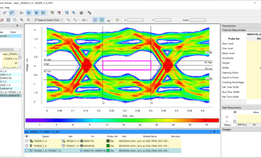
CR-8000 Design Force SI Advance integrates eye pattern analysis directly into the PCB design environment, allowing engineers to evaluate high-speed communication channels while layouts are still evolving.
Using industry-standard IBIS, IBIS-AMI, SPICE, and S-parameter models, engineers can simulate both parallel buses and high-speed serial interfaces, evaluate eye masks, inspect setup-and-hold timing, and investigate how routing decisions influence overall channel performance. Additional capabilities such as time-domain reflectometry (TDR), crosstalk analysis, and frequency-domain simulation help identify the physical mechanisms responsible for eye closure.
Because signal integrity analysis remains connected to the PCB design database, engineers can evaluate routing alternatives, investigate connector behavior, and understand the electrical impact of design changes without leaving the design environment. This shortens the feedback loop between layout and verification, enabling potential problems to be identified while modifications remain relatively inexpensive.
For increasingly complex multi-board products, this integrated workflow provides valuable visibility into complete communication channels rather than isolated PCB segments.
Designing for Reliable Communication
Eye pattern analysis has become one of the most effective methods for evaluating high-speed digital interfaces because it connects numerous signal integrity effects into a single measure of channel quality.
For PCB designers, the objective is not simply to create an eye diagram with a larger opening. It is to understand how routing decisions, stackups, vias, connectors, power distribution, and complete interconnect structures influence the performance of the finished product.
As electronic systems continue to increase in speed and complexity, successful PCB design depends on more than satisfying layout constraints. It requires understanding how the complete communication channel behaves before hardware reaches the laboratory.
By integrating eye pattern analysis directly into the design workflow, engineering teams can identify potential signal integrity issues earlier, make better-informed design decisions, and reduce the risk of costly validation failures later in development.

- Blog
September 04, 2026
Building Confidence in SERDES and DDR Performance Before Prototyping
Learn why SERDES and DDR PCB designs can pass routing checks yet fail during validation, and how earlier signal integrity and timing verification helps reduce late-stage problems.
Read now
- Blog
July 24, 2026
The PCB Passed Every Review. So Why Did the Product Fail?
PCB Design, Electronic, Blog
- Blog
May 13, 2026
Why PCB Design Has Outgrown Single-Board Thinking
Modern electronic products are no longer built around a single PCB. As systems become faster, denser, and more interconnected, engineering teams are being forced to rethink how they design, verify, and manage complex multi-board products.
Read now
- Blog
March 25, 2026
Determining Conductor DC-Resistance in CR-8000 Design Force
Explore how CR-8000 enhances PCB design with integrated control of impedance and resistance—enabling precise analysis for both high-speed and high-power applications, from signal integrity to power distribution optimization.
Read now
Related Items
- Products
September 22, 2023
Design Force SI Advance
Design Force SI Advance combines a comprehensive range of new functionalities to enhance your signal integrity analysis capabilities.
Read now
Integrated Signal Integrity Simulation and Analysis tools
- Webinar
July 06, 2020
Practical Signal Integrity for improved EMI Control in PCB Design
In our webinar we will provide an introduction to the challenges of signal integrity and the underlying physical effects. This will provide the basis for practical tips to address the related challenges during PCB design.
WATCH NOW