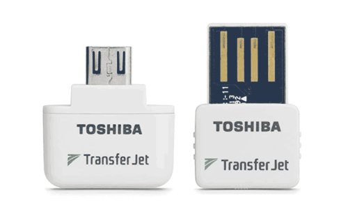
Toshiba – RF Module Shrink (TransferJet™)
Toshiba faced a difficult design problem: their TransferJet™ technology was embedded in a customer cell phone, and when the next rev of the phone came around, they learned that they needed to shrink the board from 8mm x 8mm to 4.5mm x 6mm, and they had to shrink the module thickness from 1.7mm to 1.0mm. The original design was a simple board with a wire bond package and several peripherals. Competitive pressures required a significant reduction in size and thickness. On top of that, they had to add RF matching to simplify the adoption of the module. This post describes how Toshiba used Zuken’s CR-8000 Design Force with ANSYS analysis tools to accomplish the project.
The wish list
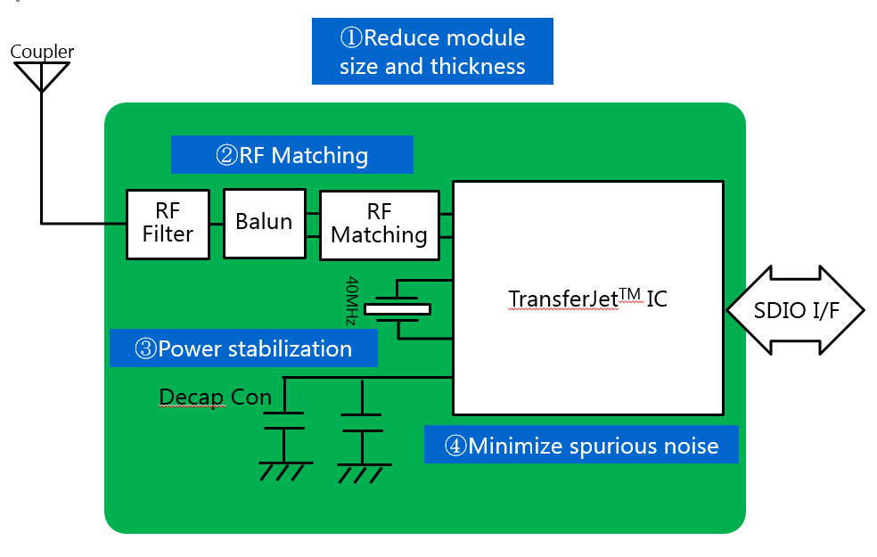
The overall goals were to shrink the size and thickness, provide RF matching and power stabilization, and to minimize noise. The system block diagram plus the design goals are shown in the image below.
To accomplish these goals, Toshiba came up with the following requirements:
- use a bare flip-chip die instead of a wire bond package
- embed the die in the package substrate, and add extra test pins
- use co-design tools and methodologies to optimize pin assignments more effectively
- use system-level co-analysis
- view and edit using 3D design capabilities
- design in close collaboration with CAE tools
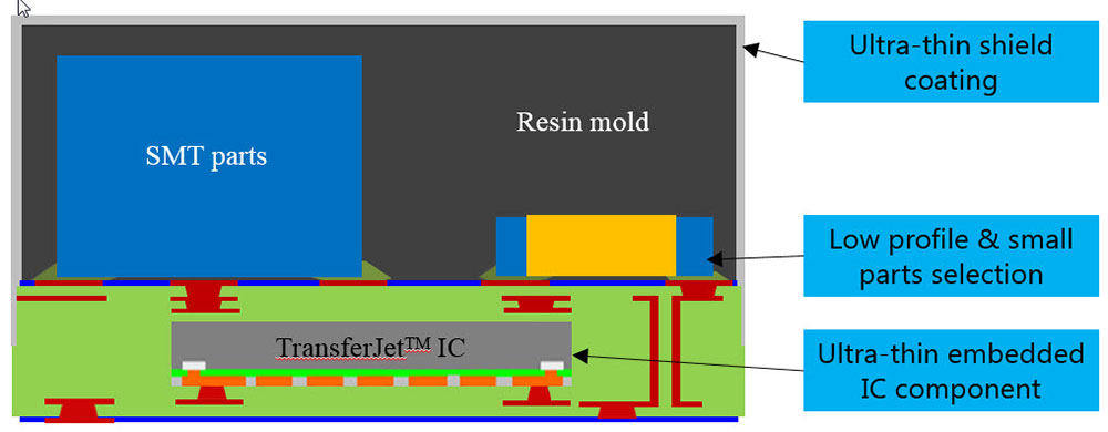
Toshiba soon discovered that Zuken and ANSYS were the only vendors who could provide tools to meet all of the functionality requirements. They began by doing some feasibility studies, taking advantage of the 3D design and embedded design functionality in CR-8000 Design Force. They embedded the die and explored putting it face up and face down and also explored the effects of adding test pins. What resulted is the configuration shown below – the die had the extra test pins, it was placed face down, embedded within the substrate, and employed ultra-thin shield coating on the package and an ultra-thin IC component.
The design process
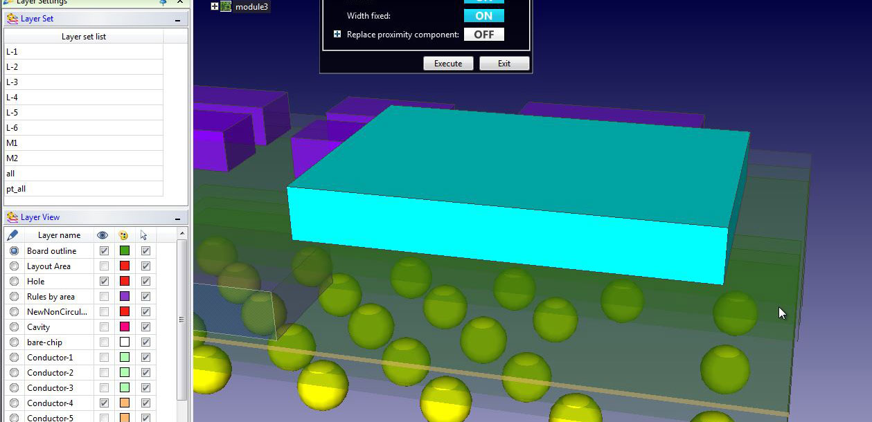
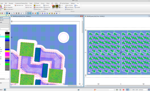
 The module was then combined with the board to form a 3D chip-module-board design view. Each device had its own design rules. Zuken’s CR-8000 Design Force enabled engineers to easily and quickly switch design context as they proceeded through the design process. When they needed to design the package in 3D, a click of a button switched to 3D mode, with another click, they were back in 2D, and with another click of a button they could design in the IC.
The movie below demonstrates the process:
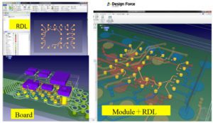
The IC RDL routing was done natively in an OpenAccess design environment using IC design rules, and generated mask-ready RDL routing. Package routing was completed with package design rules. Pin assignments were updated as needed to create the simplest and most optimal routing in both the die and the package.
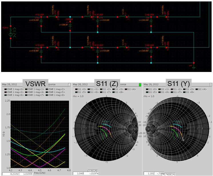
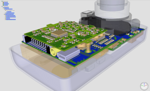
Next, a 3D model of the system was generated. This model included IC, package, and board elements for a hierarchical 3D model that was passed to ANSYS for RF matching analysis. The RLC parasitics were based on a 3D model and were passed to ANSYS Q3D analysis. The circuit and analysis results are shown below:
CR-8000 Design Force then generated an ANF file for use in Siwave for power stabilization. A port was set for each power and ground terminal of the IC and power and ground impedance analysis from the IC terminals was run. From this analysis, the optimum number and value of the decoupling capacitors required was calculated.

In order to minimize noise, engineers performed a static resonance analysis on a 3D model of the module. They found a strong resonance at 9 GHz, and were able to find the source of the resonance.
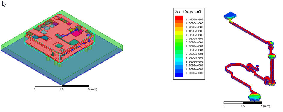
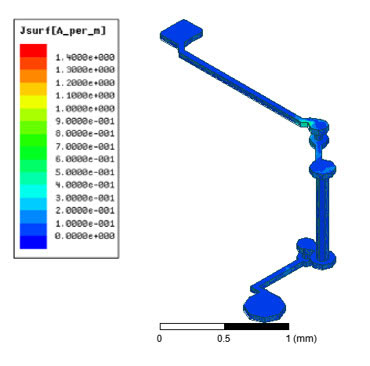
Once the resonating wire was corrected it was time to re-create the 3D model, and re-run the resonance analysis to confirm the problem was fixed.
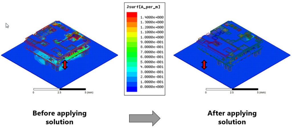
Finally, after analyzing dynamic noise, engineers found it exceeded their constraints. So from there, they built up a series of 30 possible solutions, and ran the analysis on each while applying a stimulus at the source of the noise on the IC. The software was able to identify the solution that gave the best results. reducing noise to 1/30th of the original measurement.
Now that they found good package results, they combined the module with the board for a final waveform, noise, and thermal analysis of the product and confirmed that it met the requirements.
Quick and accurate results
Toshiba was able to use CR-8000 Design Force to combine their chip, package, and board into a 3D design structure for their co-design feasibility studies to meet their physical design requirements. Tight coupling with ANSYS analysis tools enabled them to find and correct problems and complete the project.
CR-8000 Design Force is the only tool that can tightly integrate semiconductor, package, and PCB devices, and provide the tight links to ANSYS tools for quick and accurate analysis results.
For more details about the flow, see the attached file.


- Blog
Der Layer-Stack-up und die präzise Berücksichtigung der Leitungsimpedanz sind entscheidend für robuste High-Speed-Designs. Erfahren Sie in unserem Blog, wie Sie Stack-ups optimal mit CR-8000 und Polar Speedstack™ gestalten können.
- Blog
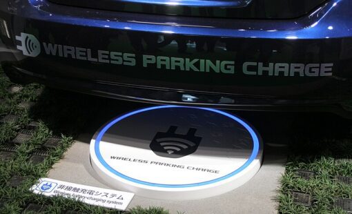
Die drahtlose Energieübertragung (Wireless Power Transfer, WPT) ersetzt Kabel und Drähte in vielen Bereichen. Die Lösungen von Zuken unterstützen Ingenieure bei der Entwicklung, Simulation und Validierung von WPT-Systemen.
- Blog
Der PCB-Markt setzt sein kontinuierliches Wachstum fort. An der Spitze dieses Wachstums steht der Sektor der Flex-PCBs. In diesem Blogpost zeigen wir Ihnen das Potenzial von Mehrfachnutzung in der Fertigung von Flex-PCB-Designs und untersuchen mögliche Kosteneinsparungen.

- Blog
Das Release 2021 von CR-8000 Design Force wartet einmal mehr mit einer Fülle von neuen und verbesserten Funktionen in der gesamten Tool-Suite auf.
Related Content
- Products
Design Force kombiniert konventionelles 2D-Design mit nativem 3D-Design und den neuesten Technologien in Benutzeroberfläche und Grafik für schnellstes Rendern und Aktualisieren.
- Anwenderbericht

- Products
CR-8000 umfasst eine Suite von Anwendungen, die den gesamten Lebenszyklus des PCB Engineerings abdecken.