
How Virtual Prototyping Tools Can Help Decide if Fan-out Wafer-level Packaging is Right For Your Product
Since it contributed to making the iPhone 7 even thinner than its predecessors, fan-out wafer-level packaging (FO-WLP) technology has risen in the collective consciousness. By adopting FO-WLP on this scale, Apple sent out a signal that though highly novel, the technology had matured.
What is Fan-Out Wafer-Level Packaging?
Put simply, FO-WLP establishes die-to-die and die-to-ball grid array (BGA) connectivity directly through packaging redistribution layers (RDLs), eliminating the packaging substrate used in more established flip-chip and wafer-level chip scale packages (WLCSP).
This type of packaging has a huge range of benefits including:
- More I/O support
- Reduced vertical footprint, by an average of 40%, allowing reduction in product form factor increase in component stacking
- Reduction in costs, by eliminating the interposer and insertion of through-silicon vias (TSVs)
- Improvements in electrical and thermal performance, as the transistors drive less metal length.
But, of course, you have to work hard to achieve these benefits. Some of the technical challenges include:
- Conducting extensive trade-off studies to determine whether the Fan-out wafer-level packaging architecture is right for the product based on: functionality, price, performance, size, weight and style.
- Integrating the normally independent design processes for the chip and package to optimize FO-WLP design, with its strong interdependencies between the chip and package.
How Do I Decide if Fan-Out Wafer-Level Packaging is for me?
To work out whether FO-WLP works for your product, or whether you would be better choosing a more established package technology, you want a design flow that allows you to carry out those exhaustive trade-off studies at the conceptual design stage. A new generation of integrated chip/package/board co-design tools, makes it possible to optimize fan-out wafer-level packaging designs to a greater degree than ever before, by considering the system-level impact of each design decision.
Zuken’s CR-8000 Design Force offers a new virtual prototyping process to enable investigation into the effects of alternative packaging approaches on functionality, price, size, weight, etc. in the early stages, without investing time into fully defining the design. The options can be evaluated collaboratively, with the ability to make trade-offs before committing to detailed design.
Here is a typical trade-off analysis process:
- Define the functional design using reuse blocks, BoM-based functional blocks or any existing detailed design, usually from the previous product generation
- Plan package technology – evaluate alternatives in the context of the overall system design. Consider the impact from functional, physical, geometric and parametric product views.
- Validate cost and weight targets, among other factors, before committing to detailed design.
Design Optimization
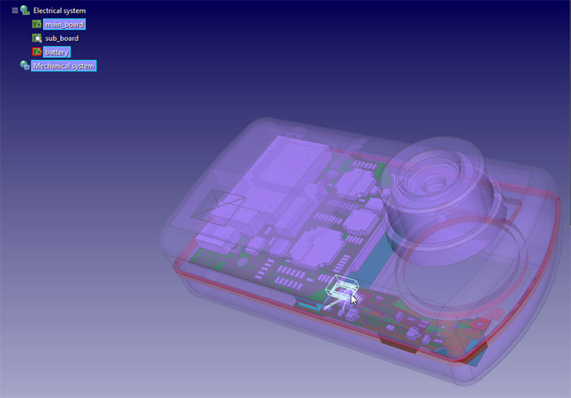
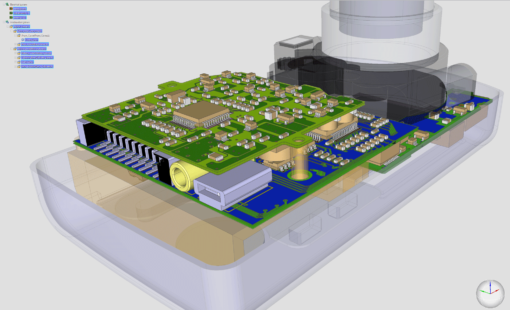
Once the basic packaging architecture decision has been made, an integrated 3D chip/package/board co-design environment makes it possible to optimize the IC, package, board and enclosure in a single view, so everyone working on the project can see their design within the context of the full product.
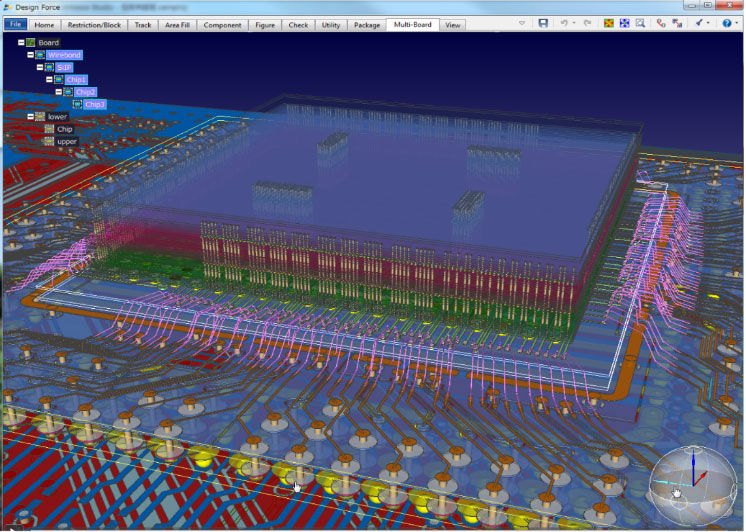
Zuken’s CR-8000 Design Force co-design environment for chip, package, and board to enable package path-finding
For example, engineers can perform a feasibility study of different numbers of package layers, while considering the routing of the RDL on the IC side and the escape route on the PCB side in a single design view.
Using system-level co-design of the chip and package makes it possible to optimize bump and ball placement, I/O placement and pin assignment to lower chip, package and PCB layer counts, even in non-traditional structures with routing complexity such as FO-WLP and WLSCP.
- For an in-depth article on this subject, see “Is Fan-out Wafer-Level Packaging Right for Your Product?” in PCD&F.
- Is Fan-out Wafer-Level Packaging Right for Your Product?

-
Solutions Architect at Zuken USA


- Blog

- Blog
Executives’ Perspectives on Digital Transformation #5
- Blog
Explore how CR-8000 enhances PCB design with integrated control of impedance and resistance—enabling precise analysis for both high-speed and high-power applications, from signal integrity to power distribution optimization.

- Blog
Build accurate dynamic cables in E3.series by defining cores, shields, and twisted pairs so schematics, reports, and formboard outputs stay consistent.
Related Content
- Products
Zusätzlich zum Multi-Board PCB Design unterstützt Design Force auch die Entwicklung von IC Packages für Wire-Bond, Flip-Chip und High-Density Advanced Packaging
- Products
Design Force kombiniert konventionelles 2D-Design mit nativem 3D-Design und den neuesten Technologien in Benutzeroberfläche und Grafik für schnellstes Rendern und Aktualisieren.

- Products
CR-8000 umfasst eine Suite von Anwendungen, die den gesamten Lebenszyklus des PCB Engineerings abdecken.