Zuken Supports Next-Generation 3D LSI-Semiconductor Mounting Design Technology
With the utilization of CR-8000 Design Force, Zuken helps to overcome design challenges associated with 3D integration in the pursuit of next-generation semiconductor technologies.
Munich, Germany, and Westford, MA, USA, December 6, 2022 – Zuken has established a partnership with the WOW Alliance headed by Professor Takayuki Ohba from the Research of Science and Technology Laboratory at the Tokyo Institute of Technology. The WOW Alliance is an industry-academia research platform that brings together various stakeholders, including companies, universities, and research institutions, with the goal of advancing the development of next-generation semiconductors using wafer-on-wafer (WOW) integration technologies.
Led by the Laboratory for Research and Technology at the Tokyo Institute of Technology, the WOW Alliance is actively involved in the advancement of a cutting-edge chiplet integration technology. The primary focus of the Alliance is to tackle the challenges associated with 3D integration, encompassing concerns such as power consumption, thermal resistance, and performance enhancement with a comprehensive solution that not only addresses these challenges but also delivers enhanced overall performance in semiconductor systems.
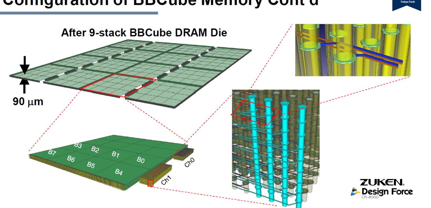
As a result of its joint effort with industry and research partners, the WOW Alliance has developed a proprietary wafer thinning technology to address the limitations of conventional wafer thickness, reducing it from the typical range of 20-30 μm to an ultra-thin 4 μm. Moreover, the alliance has also implemented a bump-less Through-Silicon Via (TSV) interconnect technology, eliminating the need for traditional bumps. Additionally, terabyte-level high bandwidth transmission is achieved through high-density super parallel interconnects, enabling the stacking of wafers in the WOW (wafer on wafer) and COW (chip on wafer) configurations.
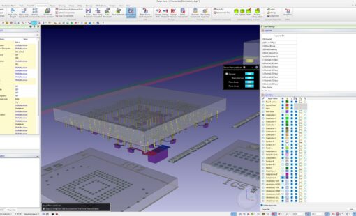
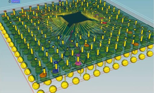
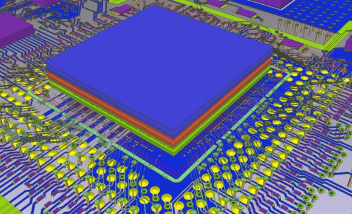
To support the design requirements of the new technology, Zuken contributes its CR-8000 Design Force multi-board design environment. This powerful design tool enables the alliance to effectively tackle the complexities of 3D integration and facilitate the design process for integrated circuits.
For more information, please visit WOW Alliance | Takayuki Ohba Laboratory, Laboratory for Future Interdisciplinary Research of Science and Technology, Tokyo Institute of Technology (titech.ac.jp)
About the WOW Alliance
Semiconductors for CPUs and memory, indispensable for personal computers and smartphones, have improved performance through device shrinkage. However, the industry is currently facing the inherent physical constraints of conventional technology when it comes to further reducing the size of semiconductor components.
To overcome these constraints, the WOW Alliance lead by the Laboratory for Future Interdisciplinary Research is developing a three-dimensional large-scale integration (3D LSI) technology using vertical interconnect technology and special ultra-thinning technology for semiconductor die stacks that is capable of improving performance while making the stacks smaller and thinner.
Using this technology, the members of the WOW Alliance are working to integrate multiple semiconductor functions into a one-stack module, surpassing the limits of shrinking devices in two-dimensions only. For more information, please visit WOW Alliance | Takayuki Ohba Laboratory, Laboratory for Future Interdisciplinary Research of Science and Technology, Tokyo Institute of Technology (titech.ac.jp)

- Blog
May 23, 2025
AI in PCB Design: From Misconception to Meaningful Assistance
AI in PCB design is increasingly seen as a game-changer, with some predicting it could soon replace entire layout teams—but this view risks overlooking both the current limits of AI and the critical expertise engineering demands. At DesignCon 2025, experts from emphasized that AI's real value lies in complementing human judgment, not replacing it. Read more on our blog.
Read now
- Press Release
May 08, 2025
Zuken Launches CR-8000 2025 with AI-Enhanced Support for High-Speed, High-Density PCB Design
Press Release
- Products
May 08, 2025
What's New in CR-8000 Release 2025
CR-8000 Release 2025 brings enhanced simulation workflows, strengthened multi-board 3D co-design, expanded AI-assisted routing, and tighter PLM synchronization
Read now
- Press Release
March 24, 2025
Zuken Joins IBM Research AI Hardware Center to Develop Next-Generation AI Hardware Solutions
Zuken has joined the IBM Research AI Hardware Center to advance 3DIC packaging, AI hardware acceleration, and EDA workflows. The partnership underscores Zuken’s commitment to driving innovation in AI-driven chip design and next-generation semiconductor packaging solutions.
Read now
Related Content
- Products
January 03, 2019
Design Force Advanced Packaging
Design Force offers an intuitive, integrated environment for designing single and multi-die packages for wire-bond, flip-chip, and high density advanced IC packaging.
Read now
IC Package and PCB Co-design
- Products
November 16, 2018
Chip-Package-Board Co-Design
In addition to advanced PCB layout capabilities, Design Force provides chip, package, and board co-design capabilities to enable real-time 3D hierarchical design. This allows design teams to concurrently create any combination of advanced die stacks, packages, and PCBs.
Read now
True co-design through hierarchical setup