Topology definition for memory buses, SerDes links, and other high-speed nets.
Architectural decisions have a greater impact on a system’s electrical quality than any later optimization. A solution that brings together topology planning, feasibility assessment, and electrical constraints already in the concept phase creates a consistent foundation for schematic and layout. Scenario EX is designed to address exactly this need.
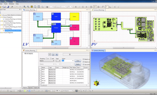
Scenario EX is an optional enhancement to CR-8000 System Planner, providing early-stage topology planning and signal-integrity awareness for high-speed interconnects. It enables architects and PCB engineers to explore routing strategies, validate feasibility, and set electrical constraints before schematic or layout begins. This supports more predictable performance and reduces downstream redesign. Scenario EX integrates directly with System Planner, allowing topology decisions to flow seamlessly into Design Gateway (schematic) and Design Force (layout), keeping design intent intact throughout the development process.
Topology definition for memory buses, SerDes links, and other high-speed nets.

Pre-layout signal-integrity estimation, helping identify risks early in the design cycle.

What-if exploration of routing strategies, layer usage, and interconnect configurations.
Scenario EX operates at the architectural level, where design freedom is highest and changes are least costly. It links functional system planning with electrical performance targets, ensuring that topology choices and interconnect strategies are aligned with real-world signal-integrity needs.
Typical applications include memory buses, SerDes channels, high-speed differential links, and multi-board connectivity.

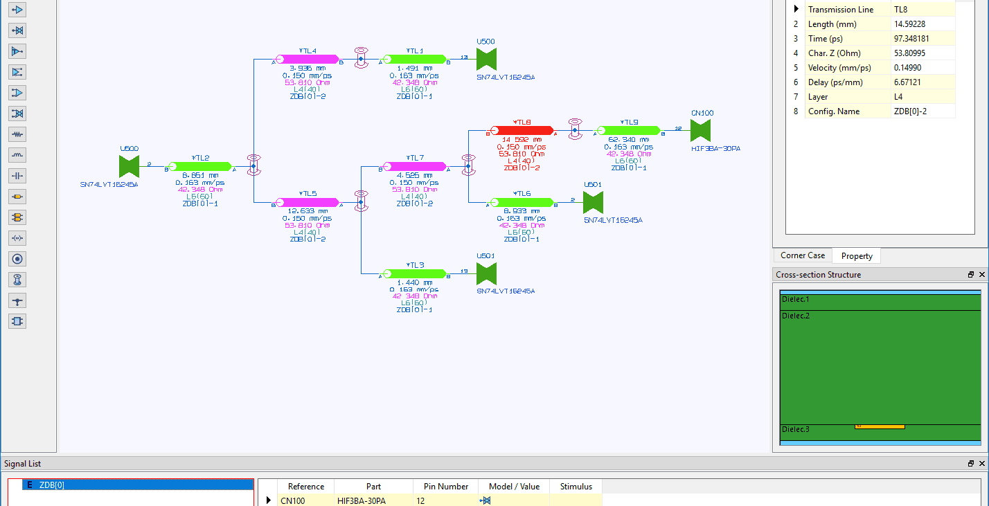
Creation and evaluation of routing strategies for critical nets, including memory buses, SerDes channels, and high-speed point-to-point links. Supported topologies include:
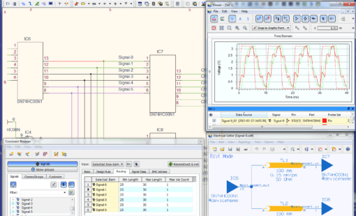
Estimation of delay, skew, and high-speed feasibility based on topology shape, segment length, and the planned stack-up, without requiring final routing geometry.
Adjustment of planned trace lengths, via counts, or layer assignments to assess how early architectural choices influence electrical behavior.
Topology results export directly into Design Gateway and Design Force as constraints. This maintains consistency from planning to implementation and reduces manual re-entry of requirements.
Scenario EX can be launched from the following products
System Planner provides a system-level design environment for the architectural planning and optimization of electronic systems and products.
CR-8000 Design Gateway provides a platform for logical circuit design and verification of multi-board system-level electronic designs.
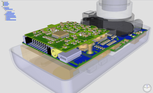
CR-8000 Design Force is the fastest, most effective PCB design solution available today. Design Force enables design teams to layout and verify their designs in the context of a complete system or product.
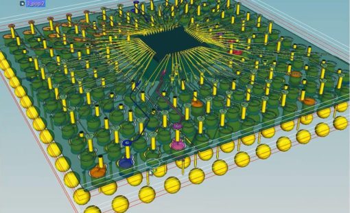
Design Force offers an intuitive, integrated environment for designing single and multi-die packages for wire-bond, flip-chip, and high density advanced IC packaging.