
Placement and Routing Hacks that Simplify PCB Designers’ Lives
The intricate interplay of electrical, mechanical, and thermal considerations, requires precise component placement, signal integrity optimization, and power distribution while navigating space constraints and ensuring manufacturability. With a number of clever tweaks and tools, CR-8000 Design Force help layout designer to maintain signal integrity and manufacturing constraints while helping simplify PCB design.
Generating Mesh Planes in an Automated Routine for Simplified PCB Design
Ensuring that the mesh planes do not interfere with signal traces, vias, or components requires careful routing planning, which may involve trial-and-error adjustments to achieve optimal results. CR-8000 Design Force now enables designers to simplify PCB design by generating mesh planes within a template area and then automatically applying them onto a conductor layer through an automated operation. When applied, the mesh planes are automatically adjusted to ensure the specified spacing between pins and tracks. The mesh is intelligently generated around tracks of adjacent conductor layers, taking into account the proximity of adjacent layers. Distancing values between tracks and mesh, providing flexibility and customization options are fully user definable.
Controlling the Automated Area Fill of Patterns Carrying No Nets
The automated filling of empty spaces on a layer with copper to create a continuous ground or power plane is frequently complicated by the presence of patterns with no nets, also known as “free copper” or “no-connect” patterns. With a newly introduced feature users of CR-8000 Design Force now can decide whether an area should be connected or left unconnected, saving valuable time and complication of manual re-work. Our video showcases three possibilities for an example containing two copper areas a) connecting both areas, b) connecting one area and excluding the other, and c) keeping both areas unconnected.
Automatically Following Existing Routing Patterns to Simplify PCB Design
Many PCB designers prefer manual routing to automatic routing because they have better control over the result from aesthetics and functionality. However, manual routing involves painstakingly aligning each new track or pair with existing traces, often resulting in misalignment, irregularities, and time-consuming adjustments. The interactive contour routing feature in CR-8000 Design Force now provides the best of both worlds: Designers can manually sketch a track or a differential pair along a designated layout area or routing pattern and automate the rest by automatically following the established pattern. This functionality allows for seamless alignment with established routing patterns, streamlining the routing process and enhancing overall design consistency, thus simplifying the PCB design process.
Just the tip of the iceberg
Icebergs are known to show only 10% to 15% of their total size above the water. The majority of the iceberg’s mass lies underwater, hidden from view. In a similar way, the features shown above just represent the tip of the iceberg in CR-8000 Design Force, by many referred to as the most advanced PCB design tool in the industry today. Visit https://www.zuken.com/en/product/cr-8000/ to find out more amazing capablities of CR-8000.

- Blog
Modern electronic products are no longer built around a single PCB. As systems become faster, denser, and more interconnected, engineering teams are being forced to rethink how they design, verify, and manage complex multi-board products.
- Blog
Explore how CR-8000 enhances PCB design with integrated control of impedance and resistance—enabling precise analysis for both high-speed and high-power applications, from signal integrity to power distribution optimization.

- Blog

- Blog
AI in PCB design is increasingly seen as a game-changer, with some predicting it could soon replace entire layout teams—but this view risks overlooking both the current limits of AI and the critical expertise engineering demands. At DesignCon 2025, experts from emphasized that AI's real value lies in complementing human judgment, not replacing it. Read more on our blog.
- Webinar
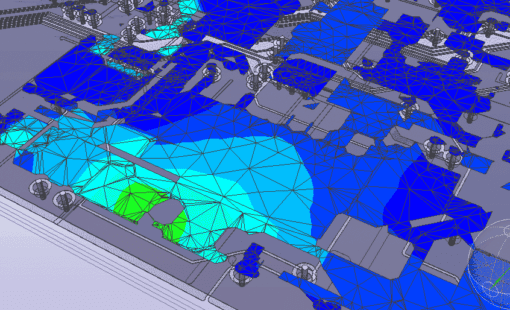
Using the example of the analysis of SerDes transmission paths such as PCI Express, SATA or USB3, we explain the methodology of an analysis- and constraint-driven assembly development with CR-8000 Design Force.
- Webinar
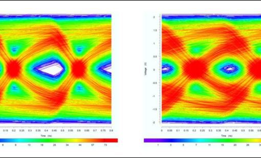
In our webinar we will provide an introduction to the challenges of signal integrity and the underlying physical effects. This will provide the basis for practical tips to address the related challenges during PCB design.