Suchergebnisse für: PCB

- Blog
As we welcome increasing numbers of IoT devices into our industries, offices and home lives, we shouldn’t be surprised to see increasing electromagnetic (EM) congestion. Or, as it’s now dubbed, the ‘Interference of Things’.

- Blog
Have you ever finished generating the manufacturing release package for the latest product design and then it occurred to you that something may be wrong? Imagine, it’s Thursday night and you just finished a nice dinner with the family. Your daughter’s soccer team won and the Broncos are playing the Chiefs tonight. It will be great to relax and enjoy the game.
- Blog
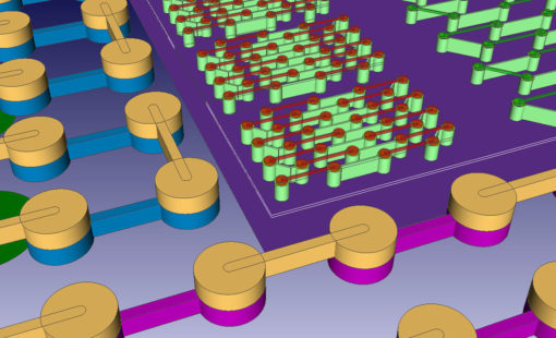
Advanced packaging techniques such as system-in-package (SiP), fan-out wafer-level packaging (FOWLP), 3D die stacks, etc. have been around for over a decade, yet with any other EDA design tool, it is still a tedious, time consuming, and error-prone process to implement these designs.
- Blog
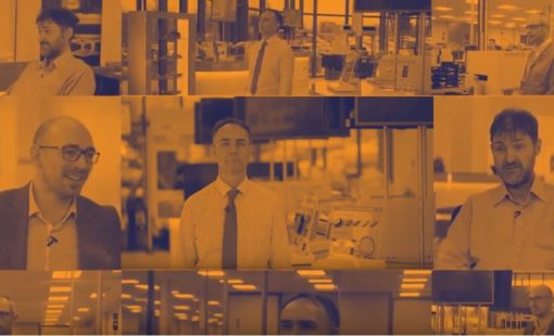
It’s not often you spend your work day laughing AND learning. But that’s how it went for Zuken Europe’s first foray into filming videos with our customers.

- Blog
Künstliche Intelligenz ist in aller Munde, seit die Medien über den KI-basierten Textgenerator ChatGPT berichtet haben. Wir haben uns mit ChatGPT ein Interview geführt.
- Products
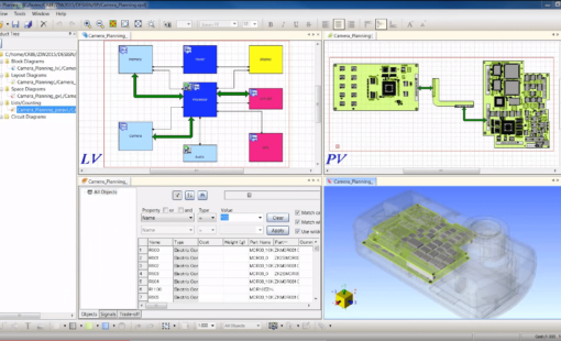
System Planner ist das erste Werkzeug, das ein vollständiges Architekturkonzept von Elektronikprodukten unterstützt. Bislang getrennte Schritte werden intelligent in einer einzigen Applikation zusammengeführt.
- Products
- Presse-Information

- Products

- Blog
Tom Lucas joined Zuken in 1997 and has been challenged in a variety of roles and rewarded with promotion opportunity. Today he is part of a small but mighty team of three specializing in PCB routing research, and is based in the Zuken Technology Centre in Bristol, UK.

- Blog
Defining initial hardware architecture requires many decisions, most of which impact a variety of different stakeholders and requirements – including multiple design tools – circuit design, PCB layout, mechanical design, spreadsheets, etc. that are used to track different elements of the design.

- Blog
Because I’ve been in the electrical/electronics (E/E) engineering industry for such a long time, I can still remember drawing PCB layouts manually. We would then work out the connection lengths of wire harnesses by laying out waxed cord lacing on a physical prototype.

- Blog
Since it contributed to making the iPhone 7 even thinner than its predecessors, fan-out wafer-level packaging (FO-WLP) technology has risen in the collective consciousness. By adopting FO-WLP on this scale, Apple sent out a signal that though highly novel, the technology had matured.
- Blog
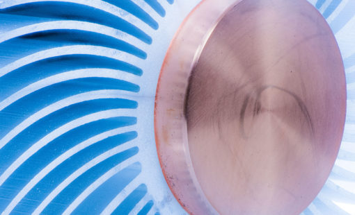
Man-carried military communication systems often consume large amounts of power. The heat must be removed from the electronics package to avoid frying sensitive electronic components. The package typically is designed to be carried in a backpack which often puts difficult constraints on the form factor and weight of the system
- Presse-Information

- Blog
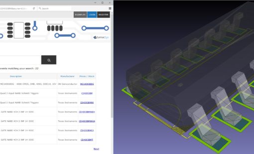
Die Aktualisierung bestehender Designs, um veraltete Komponenten zu ersetzen, ist eine zeit- und arbeitsintensive Aufgabe. Moderne PCB-Design-Tools wie CR-8000 können dabei helfen, diesen Prozess zu optimieren.