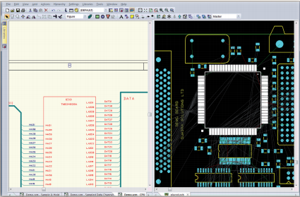
CADSTAR Placement Planner
CADSTAR Placement Planner
CADSTAR Placement Planner enables the engineer to engage the placement process during logical circuit design. Whether you are conducting placement studies for real estate planning or defining the location of critical components, Placement Planner helps improve your design flow between logical design and PCB layout.
Placement Planner is an add-on to CADSTAR Schematics, and is intended to help electronic engineers communicate their intent and provide guidance to the PCB designer more effectively, without time-consuming iterations that can cause unnecessary delays.
Top features and benefits
- Engineers can manage schematic and layout reuse blocks to improve design cycle time
- Define placement of critical components to optimize board performance and real estate early in the design process
- Constraints and high-speed requirements are defined and tested before layout to reduce costly iterations
- View and cross-probe between schematic and PCB design data to ease verification
- Access to CADSTAR’s many powerful placement features during schematic entry
Download Datasheet
