Who’s afraid of DDR4?
What IC designers do to help us route high-speed PCBs
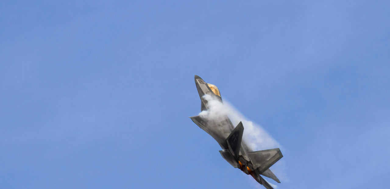
Modern military aircraft like the Lockheed Martin F-22 Raptor achieve incredible speeds and maneuverability – but during their entire flight, systems constantly check and adjust to keep them in the sky.
The speeds you get on PCI Express and other ultra-fast standards are also incredible – faster than the theoretical limit of 30 years ago. What applies to planes like these also applies to signaling: the same kinds of thinking and approach. You’d think this would make PCB layout harder, but it doesn’t have to be that way. IC designers want their devices to work well on PCBs. They help us a lot – if we know how to take advantage of it.
Shorter, smoother signal path from silicon to PCB
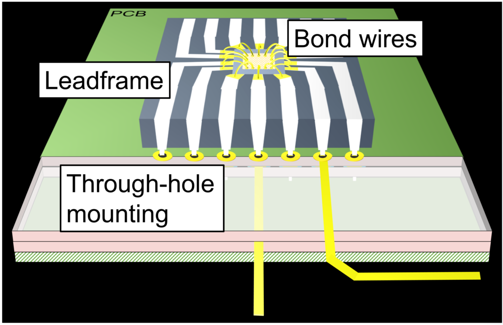
Signals on old DIP packages travelled a long and rocky road before they reached a PCB trace. With slow devices, like Standard TTL, this didn’t matter. Signals didn’t need topology or characteristic impedance control – not apart from RF circuits, and specialists designed those. Loading? Yes, but just keep trace lengths and fan-out under control and everything would be fine (Fig. 1)
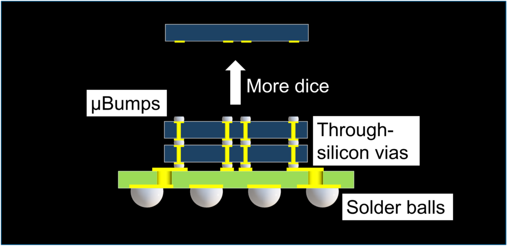
Things are different now. Look at this simplified diagram of a DDR4 SDRAM package (Figure 2): Bond wires gone; silicon flipped over; micro-bump connections to conductors on a substrate, then to solder balls that connect the chip to the PCB. More memory on each chip meant building upwards. Each layer of silicon is called a “die”. Chip designers have arranged the solder balls for our convenience, as we shall see.
What SDRAM designers did for us
Let’s look at the basics of routing DDR4 memory. The ones I’m talking about here are in 96-ball BGA packages. These devices typically connect to buses and signals in a similar way to what’s shown in Figure .
Address/command/control, differential clock and RAS/CAS signals usually connect to multiple SDRAMs in a type of daisy-chain topology called “Fly-by”. You couldn’t do that with DDR2. You had to route the clock in an “H-tree” topology to equalize the delay from source to each SDRAM. DDR3 and DDR4 added “write-leveling”, so the hardware could deal with those delays instead of PCB layout engineers. Data (DQ) and data strobes (DQS) are usually point-to-point. On a memory card, the devices are exactly evenly spaced and that’s also best for devices mounted directly on PCBs.
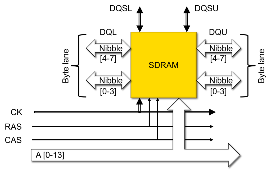
This example connects address, command and control signals together on two internal layer pairs. You can run traces directly above or below each other on non-adjacent layers because ground and power plane areas in between prevent any crosstalk. In fact, it’s good to do that, because that means you can optimize how you use routing channels. Trace lengths can be exactly equal, taking out any need for lengthening between SDRAMs. You might still need some lengthening between the controller and the start of the bus unless the controller can fix that for you.
The balls for these signals are at one end of the device (Figure ) – out of the way of the routing channels you need for data signals.
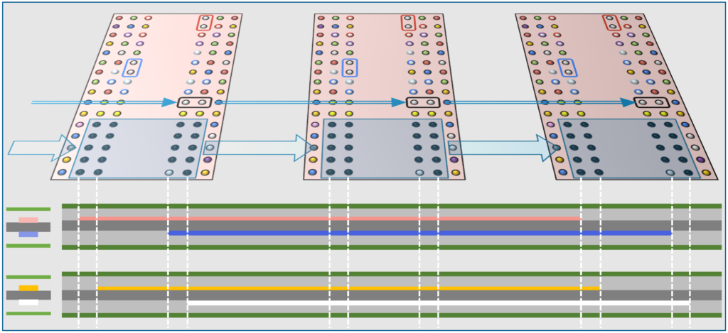
Jog the routing in the right places and you can avoid both same-layer and adjacent-layer crosstalk without adding to trace lengths (Figure ). That’s no accident – it’s clever IC design.
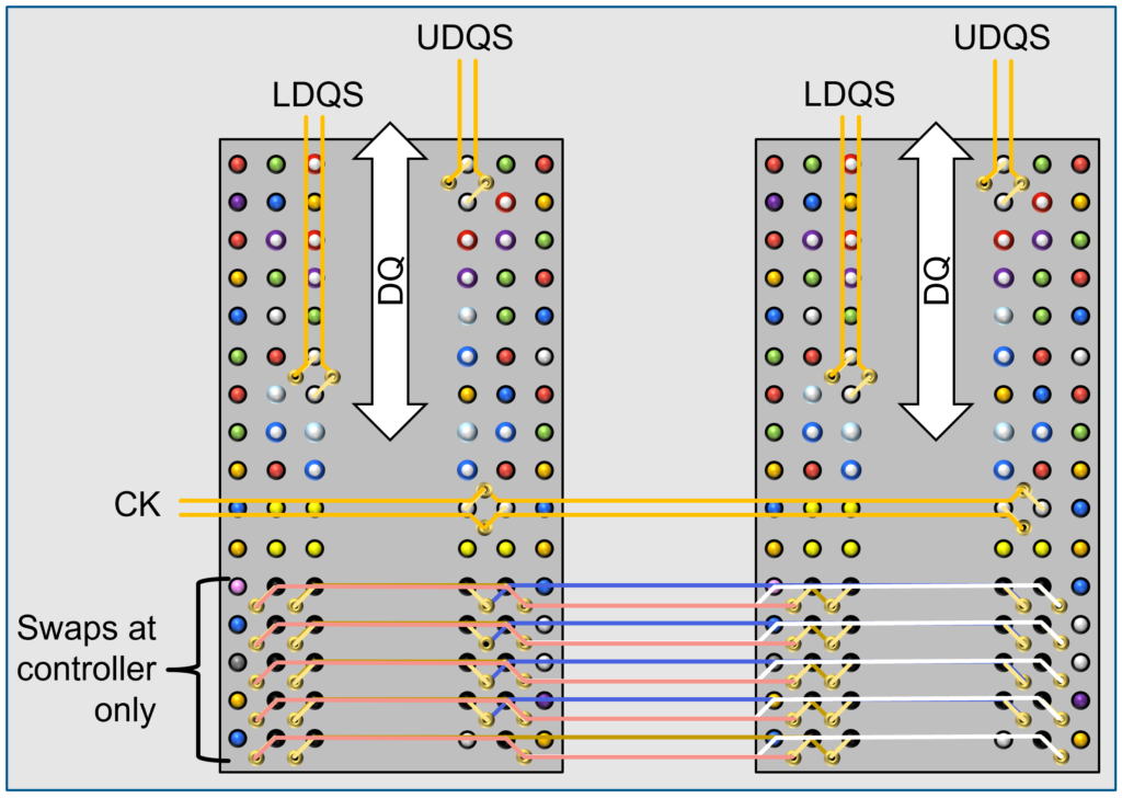
And look at the differential CK that’s routed with them. Balls for the + and – sides of the pair are in line with the routing direction. This wouldn’t seem sensible if you routed direct to the balls, but we’re routing to fan-out vias. You need lengths and via positions on the two sides of a diff pair to be equal before they go parallel. That’s essential for really fast pairs or the signals won’t travel cleanly. Because of the ball and fan-out via positions, you can equalize those ends easily. If you swap the surface-layer fan-out traces, you can fix differential trace crossovers. The differential (DQS) data strobes work the same way and they’ll run at right angles to address/cmd/ctrl, so you end up with something like Figure 5.
Ultra-fast I/O
Just as with fast jet planes, speeds you get on PCI Express and other ultra-fast standards are faster than what we used to think was the limit. To do that, IC designers went to a whole new level. They thought it through and all we have to do is to use what they’ve done for us.
Look at the FPGA I/O bank in Figure 6. The differential pair balls are at the edge of the package to minimize obstructions. The technique for routing differential pairs here is like the one for differential strobes in Figure , but these are even faster.
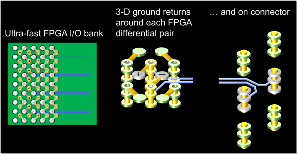
The fan-out vias are next to symmetrical ground vias either side, to provide high-speed return paths in the third dimension.
The connector is through-hole and you can see its ground return pins. Inside the connector, the conductors couple to each other and to ground returns to match differential impedance as the signals come off the flat and go down the holes.
If you change layer anywhere else, you have to include symmetrically-placed ground return vias next to any signal vias. On single-layer changes through laser-drilled build-up vias you can bend those rules, because the distance is short and the vias are tiny. In other words, you can trade production cost for density and performance. These differential pairs were routed on a single internal layer, symmetrical between two ground planes, for best signal integrity.
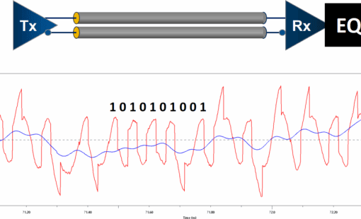
The I/O inside the FPGA is very smart. Drivers for each pair pre-distort the waveforms so that they arrive in best shape at the other end. They do this dynamically and react to conditions – even applying different changes to different parts of the same waveform.
This means signal processing directly in the hardware, more like a control system – not just on-die termination or pre-emphasis that turn up in more basic devices.
The same kinds of mathematics that land planes in fog now routinely control device I/O.
Final thoughts
Hardware gets smaller and cheaper all the time, so what high-end FPGAs do today, other devices will do tomorrow. It’s cheaper to push more data through copper than to switch to, say, optics, so it will be popular so long as designers find a way.
Differential signals go faster than single-ended, so expect more and more of those and more and more point-to-point signals.
Laying out high-speed buses has become a truly joined-up science, with both PCB and IC designers on the team.

-
Electronic Design Technology Partner

- Blog
Modern electronic products are no longer built around a single PCB. As systems become faster, denser, and more interconnected, engineering teams are being forced to rethink how they design, verify, and manage complex multi-board products.
- Blog
Explore how CR-8000 enhances PCB design with integrated control of impedance and resistance—enabling precise analysis for both high-speed and high-power applications, from signal integrity to power distribution optimization.

- Blog
High-Speed-Serial-Links wirken oft wie schwarze Magie – steigende Datenraten verstärken dieses Gefühl. Donald Telian (SI Guys) und Ralf Brüning holen die Diskussion zurück zu den Grundlagen.
- Blog
Lerne die beiden wichtigsten Grundlagen für den zuverlässigen Entwurf von High Speed Serial Links und erfahre, wie du Herausforderungen bei der Signalintegrität bei Geschwindigkeiten von mehreren Gbit/s meistern kannst.