
EMC = DRC²: The Importance of EMC Rule Checking
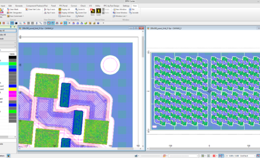
When it comes design rule checks for PCB designs, there are checks that should be performed that are just as important as spacing rules. Strict adherence to basic PCB design rule checks, such as track to track, track to via, via to via, pad to track etc. – though necessary to avoid short circuits – only scratch the surface when trying to identify potential design flaws. I often see PCB designs that are completed based on this premise and wonder what else could be hiding in the design?
DRC rules covering the verification of min and max length of routed critical signals like clicks and strobes, as well as skew differences in multi-bit buses are as important as metal spacing rules. If the minimal skew is not achieved, the PCB design will be scrapped just as easily as if shorts resulted in burning holes in the PCB during power up.
The average designer strives to meet the requirements of 100% error-free design rule checking. Many also make sure the high-speed signals are routed to proper length specification. But is that enough?
Depending on the PCB design, it may be enough. But what other DRC rules are available to help avoid basic EMC anomalies at the board level? After all, once the PCB design is assembled and powered, it now has a date with the EMC chamber. If the results are not favorable, the engineer is responsible for finding the source of the problems.
Here are some tips to help eliminate problems that may be originating in the PCB itself:
- Check for the basics like inter-layer crosstalk where tracks are routed in the same direction on adjacent layers.
- Visually examine every net while the entire PCB design is in a low light mode, looking for open and closed loops in routing patterns (again another interlayer anomaly resulting in radiation) sounds a little crazy, but it’s necessary during the layout phase.
- Ensure proper bypass capacitor placement in strict accordance with engineering know how and the manufacturer’s guidelines is crucial. That big custom ASIC or FPGA may experience a ground bounce if not the capacitor requirements are not met.
The list of potential EMC board-level problems can go on and on. The fact is, it still takes time and resources to debug a bad PCB. It may happen often enough in your company that design engineers must factor in extra time just for this process.
Solving for EMC issues within the layout is as important as completing DRC spacing checks. The more rules that are available to help identify PCB design flaws up front, the better off you are. When you’re working with a tool that provides the next level of DRC rules that focus on EMC issues, you can quickly and easily identify the rules that have flagged known issues in previous PCBs and adopt them as part of a standard PCB design playbook. PCB designers should embrace this type of rule checking, since it increases the likelihood of a successful design the first time.
Related Content
- Products
CR-8000 Advanced Design for Manufacturing (ADM) überprüft bereits in einem frühen Stadium des Konstruktionsprozesses und simultan zum Arbeitsfortschritt, ob die Entwürfe den Spezifikationen für die Montage und Fertigung von Komponenten entsprechen

- Products
CR-8000 umfasst eine Suite von Anwendungen, die den gesamten Lebenszyklus des PCB Engineerings abdecken.
- Datenblatt