advanced-ic-packaging-2

Design Force Advanced Packaging

Deal with the growing complexity in design space in handling high pin-counts
Menu

IC Package Design with CR-8000

Design Force offers an intuitive, integrated environment for designing single and multi-die packages for wire-bond, flip-chip, and high-density advanced packaging. Designers can start designs with early prototype input of chip and package data from the library, reuse data from IC layout tools, and take advantage of parametric wizards to streamline the creation of the system

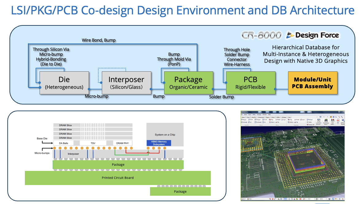
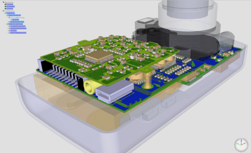
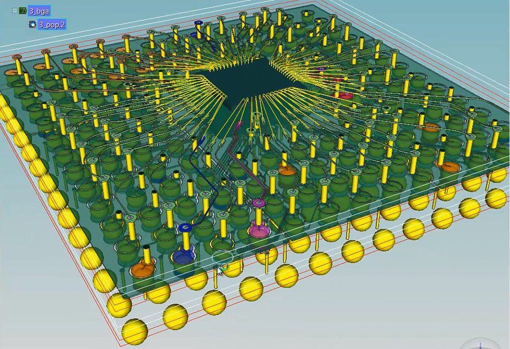
Hierarchical Co-Design for 3D-IC and Chiplet Structures

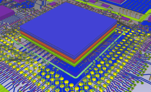
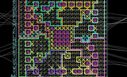
Advanced 3D-IC and chiplet designs require more than package layout in isolation. Design Force supports hierarchical co-design across dies, interposers, packages, PCBs, and mechanical data, helping teams represent the full system structure in a connected environment. This approach supports concurrent design across related objects while keeping chip, package, board, and mechanical context visible throughout the design process.

LSI/PKG/PCB Co-design Design Environment and DB Architecture

Basic-Features-for-SiP-Design-1

Multi-Object Design for Heterogeneous Technologies

Chiplet assemblies bring together different technologies, materials, and design domains. Design Force uses a multi-object design approach to support heterogeneous structures, including 3D-ICs, 2.5D silicon interposers, 2.1D RDL interposers, embedded silicon bridges, organic packages, and PCB assemblies. This helps designers manage complex package architectures without separating the work into disconnected design environments.

Tile Bump Planning for Chiplet and Flip-Chip Design

Chiplet and flip-chip package designs require careful coordination between LSI and package constraints. Design Force supports tile bump planning to help designers create bump structures that satisfy both chip-side and package-side requirements. Tiles can be saved as library data for reuse, helping teams reduce design iterations, respond to ECO changes, and support package-aware planning for high-I/O designs.

Chip I/O RDL Planning with Tile Design

Synopsys - Zuken Alliance for 3D-IC Design

Chiplet Co-Design with Synopsys and Zuken

The Synopsys-Zuken alliance supports advanced chiplet co-design workflows that connect chip-centric and system-centric design. The flow brings together Synopsys 3DIC Compiler and Fusion Compiler with Zuken Design Force for package design, interposer routing, pin assignment, package/PCB integration, and 3D integration with the package. This alliance helps support co-design across chiplets, interposers, organic packages, and PCBs.

An intuitive, integrated environment for designing single and multi-die packages

With the Design Force native 3D platform, designers can easily implement and manage dense interconnects for wire bond or flip chip packages, and incorporate embedded component technology for advanced packaging and module design

Flip-chip methodology is commonly used for high I/O count designs. This methodology greatly reduces inductance, allows high-speed signals, and possesses better heat conductivity properties.

An RDL (redistribution layer) is used to connect I/O pads to solder bumps. RDL congestion issues arise when a single layer in spite of manual routing is not enough to complete the routing for a sizable design due to sub-optimal I/O placement. Hence, in multiple die packaged systems for flip-chips, RDL routing is the key to packaging tradeoffs.

To achieve a high performance and low cost chip-package-board system, early feasibility analysis is a must to allow physical constraints to be coupled to electrical requirements. The physical constraints are used to minimize total wire-length of the RDL routes, whereas the electrical requirements are used to ensure accurate signal-power ratio, low power consumption, reduced inductance and lower thermal effects.

Designers can leverage a broad range interactive and automatic routing tools to reduce effort conducting fan-in/fan-out routing, automatic ball assignments on the package, and routing of the complete package.

Design Force supports integrations to best-in-class tools from partners such as ANSYS, AWR, Agilent and Synopsys for RF, Full Wave FD/TD, power integrity, and thermal extraction and analysis. Design Force also contains native EMI, signal and power integrity analysis for eliminating design errors.

Design Force includes an array of utilities and wizards to accurately define wire-bond profiles, bond pad placement, multi-die or bond-pad connections, managing the stacking of ICs with online design and manufacturing rule checks.

IC Package Design with CR-8000

Design Force offers an intuitive, integrated environment for designing single and multi-die packages for wire-bond, flip-chip, and high density advanced packaging. Designers can start designs with early prototype input of chip and package data from the library, reuse data from IC layout tools, and take advantage of parametric wizards to streamline the creation of the system

Unified environment

A unified environment to handle chip scale packaging (CSP), multi-chip modules (MCMs), and system-inpackage (SiP)

Automatic ball assignment with the ability to optimize complex routing solutions

Feasibility studies with advanced fan-out/fan-in and autorouting features to optimize package layer count

2.5/3D stacking structures handled in any configuration: stacked, adjacent, interposers, with wire bond and flip chip packages

Got a Question? - Contact Zuken today

For more information on how Zuken can help your design process, contact Zuken today.
Contact us today