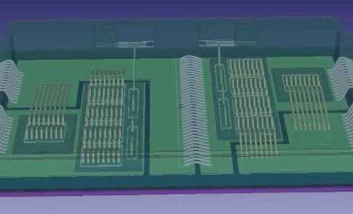
A unified environment to handle chip scale packaging (CSP), multi-chip modules (MCMs), and system-inpackage (SiP)
Design Force offers an intuitive, integrated IC package design software for designing single and multi-die packages for wire-bond, flip-chip, and high-density advanced packaging. Designers can start designs with early prototype input of chip and package data from the library, reuse data from IC layout tools, and take advantage of parametric wizards to streamline the creation of the system.
A unified environment to handle chip scale packaging (CSP), multi-chip modules (MCMs), and system-inpackage (SiP)

Automatic ball assignment with the ability to optimize complex routing solutions

Feasibility studies with advanced fan-out/fan-in and autorouting features to optimize package layer count

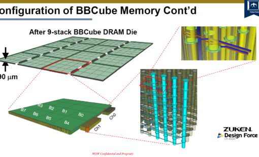
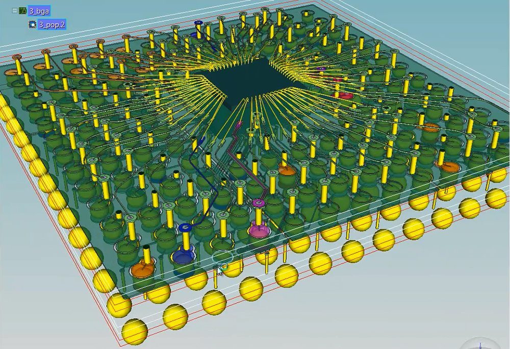
2.5/3D stacking structures handled in any configuration: stacked, adjacent, interposers, with wire bond and flip chip packages
With the Design Force native 3D platform, designers can easily implement and manage dense interconnects for wire bond or flip chip packages, and incorporate embedded component technology for advanced packaging and module design
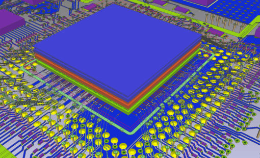
Flip-chip technology is commonly used for high I/O count designs. It greatly reduces inductance, allows high-speed signals, and possesses better heat conductivity properties.
An RDL (redistribution layer) is used to connect I/O pads to solder bumps. RDL congestion issues arise when a single layer in spite of manual routing is not enough to complete the routing for a sizable design due to sub-optimal I/O placement. Hence, in multiple die packaged systems for flip-chips, RDL routing is the key to packaging tradeoffs.
To achieve a high performance and low cost chip-package-board system, early feasibility analysis is a must to allow physical constraints to be coupled to electrical requirements. The physical constraints are used to minimize total wire-length of the RDL routes, whereas the electrical requirements are used to ensure accurate signal-power ratio, low power consumption, reduced inductance and lower thermal effects.
Designers can leverage a broad range interactive and automatic routing tools to reduce effort conducting fan-in/fan-out routing, automatic ball assignments on the package, and routing of the complete package.
Design Force supports integrations to best-in-class tools from partners such as ANSYS, AWR, Agilent and Synopsys for RF, Full Wave FD/TD, power integrity, and thermal extraction and analysis. Design Force also contains native EMI, signal and power integrity analysis for eliminating design errors.
Design Force includes an array of utilities and wizards to accurately define wire-bond profiles, bond pad placement, multi-die or bond-pad connections, managing the stacking of ICs with online design and manufacturing rule checks.
Related Resources
Zuken helps to overcome design challenges associated with 3D integration in the pursuit of next-generation semiconductor technologies.
The typical design flow for a power module is in MCAD, where only structural analysis is possible. Moving to a new design flow using CR-8000 Design Force also allows for electrical analysis too. This webinar will demonstrate the features and benefits of this new design flow.
Related CR-8000 Products
Graphical Pin Manager offers an effective FPGA / PCB co-design environment providing support for the latest devices offered by FPGA vendors
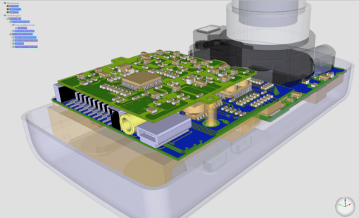
CR-8000 Design Force is the fastest, most effective PCB design solution available today. Design Force enables design teams to layout and verify their designs in the context of a complete system or product.