Using Vias to Maintain PCB Signal Integrity Featuring High-Speeds in a 3D Environment
Menu
This is the second in my series of blog posts looking at the challenge of maintaining PCB signal integrity with now-common ultra-high speeds and growing adoption of PCB design environments to design in true 3-D. Today I focus on vias and the use of return vias to overcome the issues highlighted in Part 1.
Vias explained
When traces that carry fast signals are long enough to become transmission lines, return paths are provided by inserting ground and power return planes. These planes pull the magnetic and electric field lines so that they are transverse to the direction the wave travels – a mode called TEM (Transverse Electric-Magnetic). Without TEM, things like characteristic impedance and unit-length delay are unpredictable and that means signal integrity is unpredictable too.
It goes without saying that the last thing we need is random signal integrity.
Really fast signals are often differential because differential signals yield better signal integrity and noise resistance than single-ended.
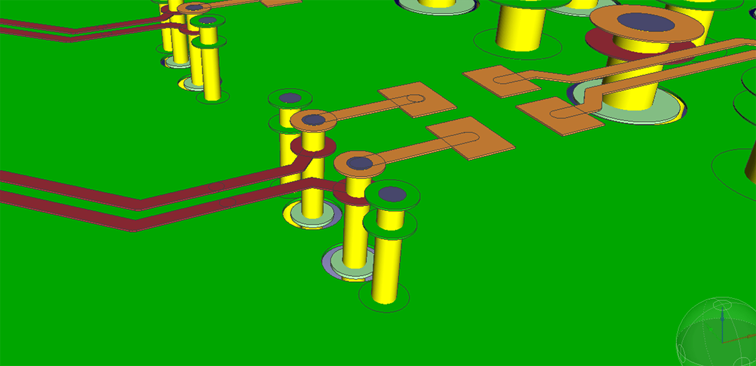
Vias connect signals in the Z dimension rather than just X and Y, but the same reasoning applies; but vias are quite complicated structures and the calculations are different.
In electronics, it doesn’t matter how a thing looks to the eye, but rather how it looks electrically.
How would we like vias to look in an ideal world?
Coaxial cables are really good for carrying high-frequency signals. They’re even better than PCB traces because they’re surrounded 360 degrees by ‘ground’. Just like the PCB ground and power plane, the shield shapes the electric and magnetic fields, but impedance and delay are easier to predict and you can even use a formula.

You can’t embed true coaxial structures in PCBs without sending the cost sky-high, but you can get near enough to this ideal without too much difficulty.
How can you make vias look like pieces of coax?
One way is to add grounded return vias at equal distances around signal vias.
An engineer did some experiments and discovered this is a good solution (details on EDN.com here).
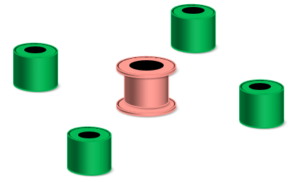 Return vias are quite expensive in terms of PCB real estate. You can use just one return via, which gets the electrical model quite close to a classic two-rod impedance calculation. It’s not quite as good, but takes up less area and has been recommended for PCI Express routing.
Other solutions
Remembering the breakpoints (from Part 1) where vias become transmission lines, the other way is to get their size under those breakpoints. That’s often more economical than adding return vias and improves performance at the same time.
Here are some popular ways:
Method: Build-up layers with small, laser-drilled vias
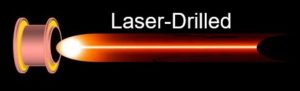
About Method: If you need build-up anyway, then keep the really high-speed routing to the build-up layers. If you don’t need it anyway, it’s quite expensive.
Method: Backdrill to remove excess via metal from through-hole vias

About Method: Increasingly popular and benefits even slower signals, where it reduces signal delay, but it isn’t suitable for fine-line BGA fanout and other delicate structures. To minimize the number of production steps, restrict high-speed routing to a group of layers beginning with an outer layer.
Method: Use Blind and Buried Vias

About Method: This can be expensive because it adds production steps. The vias have to be drilled before the layer stack is pressed. You have to plan routing layers carefully because you can drill buried vias through hard laminate, but not through soft, pre-cured PrePreg.
It goes without saying that you can avoid all these issues by restricting routing to a single layer. There is a strong trend in this direction because the latest high-speed signals are mostly routed point-to-point.
In the next and final part, I’ll show what this looks like when you’re designing a real PCB.
Also see:

-
Electronic Design Technology Partner

Jane Berrie is an EDA product innovator and technical marketing content creator, focusing on high-speed design and signal integrity. She is a published author of technical articles and a past session chair at the annual Design Automation Conference (DAC). Jane enjoys managing themed charity events, disco and going out with friends.

- Blog
May 23, 2025
AI in PCB Design: From Misconception to Meaningful Assistance
AI in PCB design is increasingly seen as a game-changer, with some predicting it could soon replace entire layout teams—but this view risks overlooking both the current limits of AI and the critical expertise engineering demands. At DesignCon 2025, experts from emphasized that AI's real value lies in complementing human judgment, not replacing it. Read more on our blog.
Read now

- Blog
February 13, 2025
The Future of Augmented Reality
Our new post explores the potential of augmented reality (AR) to transform everyday experiences in shopping, education, and navigation. It highlights how enhanced AR devices will offer immersive, interactive environments that blend the virtual and physical worlds.
Read now

- Blog
January 30, 2025
The Top PCB Design Trends to Watch in 2025
The field of PCB design continues to evolve as advancements in technology and shifting market demands push the boundaries of what’s possible. By 2025, several key trends are set to shape the industry. Find out more on our blog.
Read now

- Blog
January 23, 2025
Supply Chain Risk Management in PCB Design with SiliconExpert and CR-8000 Integration
Supply chain risk management is critical for electronics design. By integrating SiliconExpert with CR-8000, engineers gain tools to streamline component selection, manage obsolescence, and ensure design continuity. This integration supports efficient workflows, reduces costs, and mitigates supply chain disruptions.
Read now
