
Lower Manufacturing Costs with XJTAG’s New Design Gateway Plugin
![]()
JTAG is a powerful tool for debugging boards, in-circuit programming of FLASH/FPGA devices and for boundary scan. JTAG can be used to debug your first piece of hardware straight through to the high-volume manufacturing process. But let’s talk about the boundary scan side of JTAG in this post. As products get smaller and printed circuit boards become more dense, the boundary scan function becomes more and more important. Why? Because the physical space requirements for test points, ideally 0.035″ to 0.045″(.89mm to 1.14mm), is simply not available. Another factor to consider is the high pin count BGA where soldering 100s or 1000s of pins can easily create shorts or opens. These faults can stop a board from ever getting to the functional test phase for debug. So, in a nutshell, boundary scan is a tool you should consider part of every design.
Simply put, a boundary scan test shifts in a series of 1s and 0s through a predefined path or chain that enters and exits the board at the JTAG connector. A large number of ICs support a boundary scan chain so those 1s and 0s shift from pin to pin on each JTAG supported device. And with some creative test coverage schemes, even devices that don’t support JTAG can benefit. The difference between the input pattern and output pattern at the JTAG connector can identify shorts or opens on the PCB.
On the manufacturing test floor, a good portion of a board needs to be operational to get to the functional test phase. And if you have a dead board (i.e., won’t boot) boundary scan can quickly and precisely identify the fault(s) preventing a boot. Dead boards are costly and boundary scan can make a dead board operational.
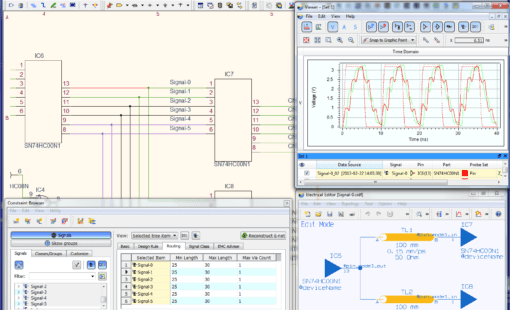
XJTAG has partnered with Zuken create a new plugin for Design Gateway and is offering it free of charge. The plugin, called XJTAG DFT Assistant, helps to validate correct JTAG chain connectivity, while displaying boundary scan access and coverage onto the schematic diagram through full integration with Design Gateway. So if you are using boundary scan today or want to incorporate it in your next design, the XJTAG DFT Assistant plugin is a tool you should be using. If you want to learn more or get the plugin, visit www.xjtag.com/zuken.

-
Vice President of Marketing, Zuken USA, Inc.


- Blog
Modern electronic products are no longer built around a single PCB. As systems become faster, denser, and more interconnected, engineering teams are being forced to rethink how they design, verify, and manage complex multi-board products.

- Blog
Explore how CR-8000 enhances PCB design with integrated control of impedance and resistance—enabling precise analysis for both high-speed and high-power applications, from signal integrity to power distribution optimization.

- Blog

- Blog
AI in PCB design is increasingly seen as a game-changer, with some predicting it could soon replace entire layout teams—but this view risks overlooking both the current limits of AI and the critical expertise engineering demands. At DesignCon 2025, experts from emphasized that AI's real value lies in complementing human judgment, not replacing it. Read more on our blog.
Related Content
- Products
CR-8000 Design Gateway provides a platform for logical circuit design and verification of multi-board system-level electronic designs.

- Products
CR-8000 is a System-Level PCB & IC Package Design software including 3D Multi-board, Analysis and MCAD Integration

- Press Release