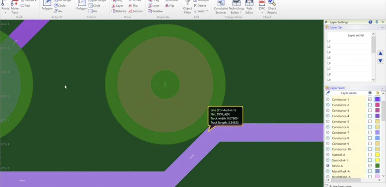
Tech Tip: Design Force Cut Land
When design space is at a premium, sometimes traces can be at risk of being exposed by any misregistration of the solder mask. If you have this situation use the “Cut Land” option under the Track tab in Design Force. Select the Cut Land option, select your Cut Targets. Make the Solder Mask layer your active layer, turn on “Edit Internal Component”, select the pad you want to cut.

-
Applications Engineer


- Blog
Modern electronic products are no longer built around a single PCB. As systems become faster, denser, and more interconnected, engineering teams are being forced to rethink how they design, verify, and manage complex multi-board products.

- Blog
Explore how CR-8000 enhances PCB design with integrated control of impedance and resistance—enabling precise analysis for both high-speed and high-power applications, from signal integrity to power distribution optimization.

- Blog

- Blog
AI in PCB design is increasingly seen as a game-changer, with some predicting it could soon replace entire layout teams—but this view risks overlooking both the current limits of AI and the critical expertise engineering demands. At DesignCon 2025, experts from emphasized that AI's real value lies in complementing human judgment, not replacing it. Read more on our blog.
