
Tech Tip: Using Enhanced Reinforce Via Functionality to Add Shielding Vias in CR-8000 Design Force
In her recent blog post, Sandy Jones introduced the new reinforce via functionality in CR-8000 Design Force. Here is one very useful application of that new functionality.
Design Force features an option to shield signals when creating their routes. The shield option automatically inserts shielding side by side, above and below, or on all four sides of the signal being routed. Figure 1 shows a signal (blue trace in the middle) shielded on all four sides by the green conductors, which are connected to the ground.
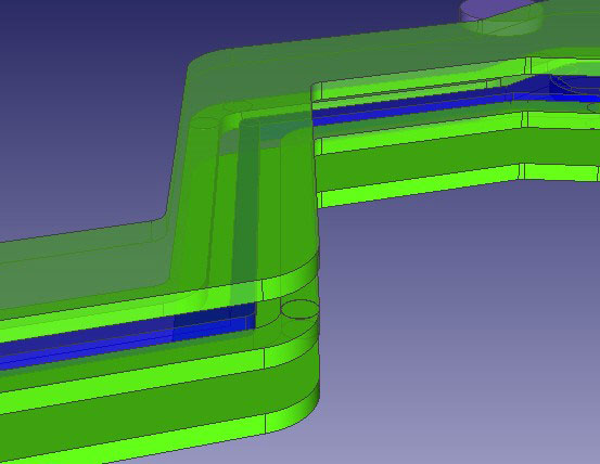
The 2018 Reinforce Via command now makes it simple to finish the shielding by adding vias all around the perimeter of this structure. On the ribbon, select the Track tab and locate the Padstack function. The Padstack function is also available in the Home tab. In the form that opens, select the option for Reinforce Via. As you’ll see in the parameters dialog, there are options to generate via patterns inside only, outside only, and both inside and outside. To generate the shielding vias, select the outside only option.
In the movie below, I specify various gaps between via centers, and I specify a distance of .015mm from the edge of the shield conductor to the via center. I then select the top and bottom layers and an image of the via pattern is shown. I can modify the pitch value to see what it looks like. Once I’m happy with the results, I click Execute to generate the vias.


- Blog
Discover how CR-8000 and Polar Speedstack™ enhance high-speed PCB stack-up design by optimizing impedance control and manufacturability for improved performance.
- Blog
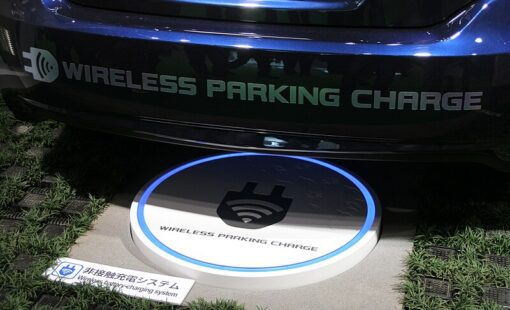
Wireless Power Transfer (WPT) is replacing cables and wires in consumer electronics, electric vehicles (EVs), and healthcare. Zuken offers a suite of solutions that help engineers design, simulate, and validate WPT systems. Learn more.

- Blog
A trend towards low power design prevails in the electronics industry today and is not likely to change in the near future. This development is driven by many reasons but primarily by the performance and storage density demands of mobile devices, where a reduction of the power consumption is crucial to extending battery life without sacrificing the bandwidth. This comprehensive guide helps you mitigate LPDDR4 Design.
- Blog
Back drilled vias: Save cost on buried vias and control cross talk.
Related Content
- Products
CR-8000 Design Force is the fastest, most effective PCB design solution available today. Design Force enables design teams to layout and verify their designs in the context of a complete system or product.

- Products
CR-8000 is a System-Level PCB & IC Package Design software including 3D Multi-board, Analysis and MCAD Integration

- Blog
In the 2018 release of CR-8000 Design Force, an amazing new improvement has been made to reinforce via. In the video below, I’ll demonstrate how this cool new feature works.