Tech-Tip: 2-Re-use Blocks in System Planner
Believe it or not, you can use your Circuit Block Library for architectural planning too!
Traditional wisdom dictates that a circuit block library can only be used for detail circuit design. The truth is that the proper toolset and solid creative thinking will also give you the same productivity boost, product reliability, and cost benefits at the architectural planning phase too.
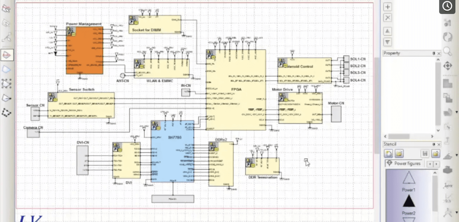
Developing electronic sub-system architectures
The odds are that several to many of the functions you need have already been designed and the ability to tie these sub-system functions to the appropriate logical modules is key to making this happen.
- Access to the same circuit block library that is used by detail design engineering is an absolute must.
- The library needs to be managed:
- Approval control
- Read/write access control
- Easily searchable
- Your architectural planning tool needs to understand the linkage between the function and logical module.
- You need the ability to directly interrogate each logical module for signal interconnects.
- The ability to export a “start point” schematic is a huge advantage.
The video that follows will walk you through:
- How to create a functional block and link it to a circuit block module in the library.
- Interconnecting signals between functional blocks.
- Exporting hierarchical and flat “start point” schematics.
Remember to stay tuned to the Zuken Blog! There is more to come on a similar topic.

-
Senior Technical Fellow


- Blog
Modern electronic products are no longer built around a single PCB. As systems become faster, denser, and more interconnected, engineering teams are being forced to rethink how they design, verify, and manage complex multi-board products.
- Blog
Explore how CR-8000 enhances PCB design with integrated control of impedance and resistance—enabling precise analysis for both high-speed and high-power applications, from signal integrity to power distribution optimization.

- Blog

- Blog
AI in PCB design is increasingly seen as a game-changer, with some predicting it could soon replace entire layout teams—but this view risks overlooking both the current limits of AI and the critical expertise engineering demands. At DesignCon 2025, experts from emphasized that AI's real value lies in complementing human judgment, not replacing it. Read more on our blog.
Related Content
- Products
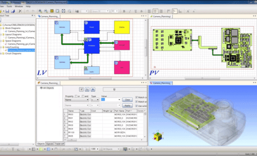
System Planner provides a system-level design environment for the architectural planning and optimization of electronic systems and products.

- Products
CR-8000 is a System-Level PCB & IC Package Design software including 3D Multi-board, Analysis and MCAD Integration
- Datasheet