PCB design

- Blog
Modern electronic products are no longer built around a single PCB. As systems become faster, denser, and more interconnected, engineering teams are being forced to rethink how they design, verify, and manage complex multi-board products.

- Blog

- Blog
Learn how the Zuken CR-8000 and Zuken E3.series can be leveraged for promoting technological advancements in renewable energy by addressing key challenges facing sustainable energy innovations.
- Blog
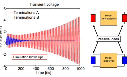
Learn the history of S-parameters/Touchstone, its advantages and disadvantages, and how to use an automated tool to overcome common challenges in your PCB design.
- Blog
PDN impedance is becoming more and more of a headache for PCB designers as IC vendors are defining increasingly tight so-called ‘target impedance limits’. This article explains what PDN impedance means for PCB designers and what to pay particular attention to.

- Blog
Since 2012, the FED has been honoring outstanding designers with the PCB design award. One of this year's winning designs was even into space.
- Blog
The benefits of developing all boards of a system concurrently on a single CAD canvas. Stacking PCBs, as opposed to connecting with cables, in multi-board design is a current and highly popular trend, as manufacturing costs are reduced and reliability improved.

- Blog
Double Data Rate 5 (DDR5) is the next-generation standard for random-access memory (RAM). The new specification promises to bring chips that have much higher performance than the existing DDR4 modules, as well as lower power consumption. Let us show you how you can be first to market with DDR5!
- Blog
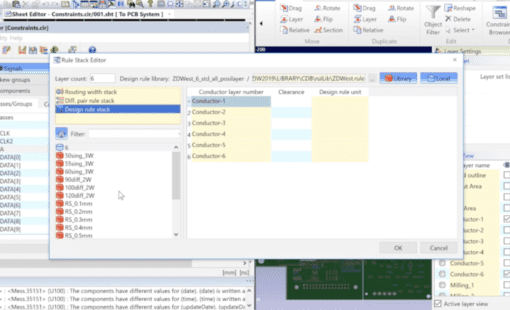
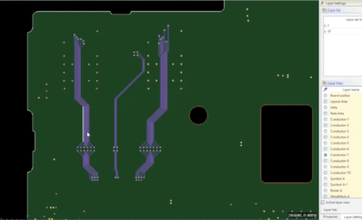
When a design requires specific minimum spacing between net classes, these clearance classes can easily be created and assigned in CR-8000 Design Gateway.

- Blog
To keep a good high-speed signal quality from driver to receiver on a PCB is not an easy task for designers. One of the most challenging issues is managing the propagation delay and relative time delay mismatches. Let me take you through the process...

- Blog
Every day, more and more of our lives become connected with IoT technology. With billions of smart products already out there.
- Blog
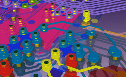
PCB design tools were built on 2D software methods in the 1980s. Many of today’s design tools still use that 2D code base. Mechanical tools have moved on to native 3D design. PCB has been stuck more or less in the 2D world. Extensions to the 2D code base made 2.5D and 3D visualization possible. But designing in 3D requires the tool to be built on a 3D kernel.

- Blog
PCB designers working with advanced and complex designs are constantly pushing the boundaries to satisfy the signal integrity of routed differential pairs and busses. Those who work with flexible and flex-rigid PCB designs are perhaps the most demanding of all. A while ago, the introduction of the curved corner style for routing trunks in CADSTAR made a big difference to this group of users.
- Blog
In this tech tip, we will explore how you can clear a routed trace pattern on multiple conductive layers. Watch our video to go through the steps with us.
- Blog
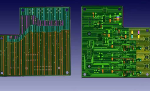
Sometimes, engineering requirements force designers to swap the position of conductive layers in a board stackup. With CR-8000 Design Force, you can do this simply and quickly by using the Restriction/Block functions.