Tech Tip: Routing a PCB design in a native 3D Tool
 PCB design tools were built on 2D software methods in the 1980s. Many of today’s design tools still use that 2D code base. Mechanical tools have moved on to native 3D design. PCB has been stuck more or less in the 2D world. Extensions to the 2D code base made 2.5D and 3D visualization possible. But designing in 3D requires the tool to be built on a 3D kernel.
3D visualization of a PCB is essentially available in every PCB design tool on the market. However, 3D visualization is not a 3D design. Placing components on a PCB in a 3D view using accurate shape 3D models is 3D design. Another aspect of a 3D design is design rule checks for both collision and clearance utilizing 3D models of the components and the PC board enclosure. 3D design requires a 3D kernel that replaces the 2D modeling code base. Let’s get back to the purpose of this blog – native 3D routing.
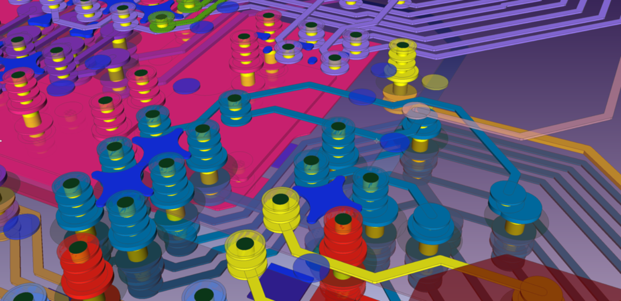
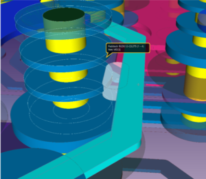
Have you tried it? The ability to fan-out micro vias under extremely small BGA footprints is difficult enough in a 2D topside view. The overlay of graphics primitives of filled lines and circles can be quite frustrating.
There are those tools that allow designers to quickly toggle from 2D routing to 3D views for a quick visualization only to have toggle back and forth to make the small adjustments to get the via placement just right.
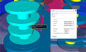
What if you could route in 3D? Since the introduction of Zuken’s CR-8000 Design Force, users have been able to realize native 3D placement and routing. In fact, when we asked Design Force users how much time they spend actually routing in 3D versus 2D, the average response came back at approximately 45%. 2D design is very different from 3D and involves change. Not every PCB designer has decided to dive into 3D design mode.
Let’s take a look at some of the benefits of 3D routing that might change your mind.
- Real-time Visualization with transparency

- Less cycle picking to select the desired item.
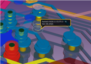
- Immediate DRC response.
- Take actions in 3D like trimming pads on specific layers
With Powerful 64 bit graphics equaling those used in modern gaming technologies PCB Designers can grow and become more efficient in their day to day placement and routing challenges.
If you have not experienced true 3D placement and routing, you should. You have to give it a try!

- Blog
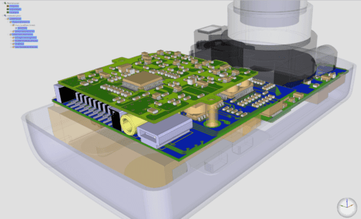
Modern electronic products are no longer built around a single PCB. As systems become faster, denser, and more interconnected, engineering teams are being forced to rethink how they design, verify, and manage complex multi-board products.
- Blog
Explore how CR-8000 enhances PCB design with integrated control of impedance and resistance—enabling precise analysis for both high-speed and high-power applications, from signal integrity to power distribution optimization.

- Blog

- Blog
AI in PCB design is increasingly seen as a game-changer, with some predicting it could soon replace entire layout teams—but this view risks overlooking both the current limits of AI and the critical expertise engineering demands. At DesignCon 2025, experts from emphasized that AI's real value lies in complementing human judgment, not replacing it. Read more on our blog.
Related Content
- Products
CR-8000 Design Force is the fastest, most effective PCB design solution available today. Design Force enables design teams to layout and verify their designs in the context of a complete system or product.

- Products
CR-8000 is a System-Level PCB & IC Package Design software including 3D Multi-board, Analysis and MCAD Integration