
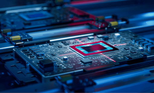
Printed circuit board shot into space
Since 2012, the FED has been honoring outstanding PCB designers with the PCB design award every two years. Zuken is once again a proud partner of the award. This year’s winners impressed with extraordinary designs. One of them was even shot into space.
![]()
The complex and demanding job of PCB designers often lacks sufficient recognition. A great designer needs to draw knowledge from many areas and acts as the link between development and production. He must translate the specifications of the circuit diagram into a design suitable for production. Not only does he have to master electrical and production engineering, but he also has to have a grasp of the fundamentals of materials science and keep an eye on countless standards and guidelines. Not to mention the consideration of the economic effects of his layout.
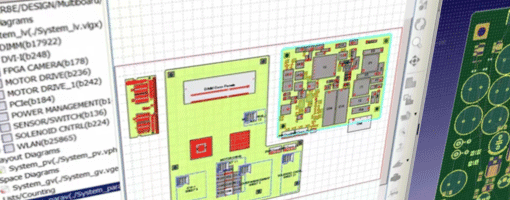
PCB Design Award 2020 Winners
In the category, 3D/Building Space Thomas Blasko from CiBOARD electronic won first place. This category focuses on the mechanical challenges that require complex, rigid, rigid-flex, or flexible circuits. With this in mind, Blasko’s project describes a system for laser scanner position measurement. The flex-rigid PCB consists of nine individual functional groups with a base area of 29mm diameter – with an integrated assembly as large as a 35mm film can.
The circuit board folds around a given aluminum milling body. The transfer of the measurement data and the power supply runs through a single coaxial cable. The big challenge here was to meet the tough mechanical specifications by cleverly partitioning the individual functions such as sensors, connectors, FPGA controller, and power supply.
Georg Scheuermann from TQ-Systems came out on top in the category high wiring density/high density interconnect (HDI). This category deals with circuits with extremely high integration density or very high transmission rates.
Scheuermann convinced the jury with his complex design. A Computer-on-Module with various high-speed interfaces and two memory blocks with 18 DDR4 memory chips each. For the supply of the memory and cores, the designer has to consider currents of up to 70 A at frequencies of up to 2.2 GHz. The cleverly designed 18-layer PCB ensures high-speed requirements and the optimal supply of processor and memory. In spite of containing a minimum number of pressings.
PCB shot into space in minisatellite
Michael Matthes from WITTENSTEIN cyber motor is the winner in the category of special creativity. In this category, the design award goes to “a rather unique solution”. In other words, a design that is particularly clever or elegantly solved, even independently of the underlying materials.
Matthes’ design enables the alignment of nanosatellites in low Earth orbit. Extremely compact – on a square installation space the size of a sugar cube – the Reaction Wheel was designed especially for the harsh space conditions. Furthermore, the square design enables space-saving integration and also offers maximum flexibility in application.
Michael Matthes has undeniably succeeded in meeting the high requirements in this category with a sophisticated layer structure of a 6-layer rigid-flex PCB. His project result is now facing the test. With the rocket launch in Baikonur, the installed circuit board was shot 600 kilometers into space in a miniature satellite.
“We are very happy about the high level of entries”, summarizes Erika Reel, president of the jury for the PCB design award. “All in all, the works show a high degree of creativity in planning and cleverness in implementation”.
Learn more about Zuken’s comprehensive solutions for PCB design.


- Blog
Modern electronic products are no longer built around a single PCB. As systems become faster, denser, and more interconnected, engineering teams are being forced to rethink how they design, verify, and manage complex multi-board products.
- Blog
Explore how CR-8000 enhances PCB design with integrated control of impedance and resistance—enabling precise analysis for both high-speed and high-power applications, from signal integrity to power distribution optimization.

- Blog

- Blog
AI in PCB design is increasingly seen as a game-changer, with some predicting it could soon replace entire layout teams—but this view risks overlooking both the current limits of AI and the critical expertise engineering demands. At DesignCon 2025, experts from emphasized that AI's real value lies in complementing human judgment, not replacing it. Read more on our blog.
Related Content

- Webinar
DDR5 is the latest generation of memory. In this joint webinar with Keysight Technologies, we’ll begin with pre-layout simulation, then transition to CR-8000. The design will then be verified by Electromagnetic (EM) simulation and system simulations in Keysight ADS, in order to build confidence in the final DDR5 design.
- Webinar