Transitioning from Architecture Design to Detailed Design
On-demand webinar
This webinar is Part 3 of a 3 part series covering the systems engineering process of converting product or system requirements into a viable and robust hardware architecture and then moving that architecture directly into detailed design without any manual re-entry.
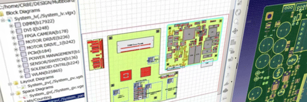
Architecture design is typically done with a variety of tools including Excel and Visio. Once an architecture is defined using these tools the architecture design must be realized in the detailed design process. That transition today is manual and error prone involving data re-entry.
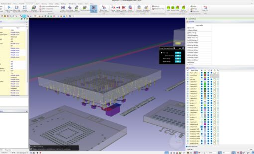
This webinar demonstrates the seamless transition from architecture design and optimization to detailed design. After a short review of architecture optimization and validation, the design will be moved to detailed design. A functional block diagram becomes a detailed design schematic or schematics. 2D multi-board planning becomes a 2D/3D PCB design ready for detailed placement and routing. Data re-entry is not required.
What you’ll learn:
- How to easily transition from architecture design to detailed design without any data loss or re-entry
- Functional block transition to a traditional schematic or schematics
- 2D multi-board floor planning transitions to a multi-board system
Who should watch:
- Hardware engineers
- System architects
- Design engineers
- Electronic engineers
- Product managers
- Engineering managers
Related resources

- Press Release
Valeo and Zuken are partnering through the Zuken Valeo InnoLab to create an open, AI-assisted electronic design platform for automotive engineering. The collaboration combines Zuken’s AI architecture with Valeo’s AI Agents and industrial expertise to reduce design times, strengthen digital continuity, and support robust electronic design across the full design flow.
- Press Release
Zuken Inc. has joined the JOINT3 consortium—an industry co-creation platform led by Resonac to accelerate the development of next-generation semiconductor packaging materials, equipment, and design tools for panel-level organic interposers—where Zuken will contribute its CR-8000 Design Force expertise to help demonstrate, optimize, and evolve design and manufacturing processes that address the growing demand for 2.xD and 3D semiconductor packages in applications such as generative AI and autonomous driving.
- Press Release
- Press Release
Zuken has joined the IBM Research AI Hardware Center to advance 3DIC packaging, AI hardware acceleration, and EDA workflows. The partnership underscores Zuken’s commitment to driving innovation in AI-driven chip design and next-generation semiconductor packaging solutions.