Next Generation Additive Manufacturing
Yes, it is true that even today, so many years after 3D printing started to garner attention and acclaim, rapid prototyping remains the single most common use for 3D printers. 3D printers offer the innovator advantages in the form of shorter turnaround times, improved development secrecy and greater design freedoms. But…it is also true that 3D printing isn’t going to remain as a tool for primarily rapid prototyping for much longer.
Enter next-generation additive manufacturing
 Anyone keeping abreast of events in the worlds of design, construction, manufacturing, or medicine will be keenly aware of the impact of additive manufacturing in these fields. There are certain products that have been rapidly affected by the arrival of additive manufacturing, prime examples are hearing aids and dental aligners. Both of these markets have been transformed by the adoption of 3D printing technologies; additive is now the default manufacturing technology for such products.
Right now, the emergence of additive manufacturing as a way to make final parts correlates well with products that require:
- Customization (where individualization is a priority, such as dental aligners and hearing aids)
- Small volumes (where scaling to mass production is not a priority)
- Difficult logistics (distributed in-situ manufacturing such as in space or other remote locations)
- Highly complex parts that cannot be made using traditional methods (such as GE’s advanced jet-nozzles)
The arrival and evolution of additive manufacturing in the mechanical world is something that people are now familiar with. The fact that it is beginning to have a similar impact in other domains of application such as medical and electrical functionality is now becoming more obvious. The underlying advantages remain the same, but the systems and materials required to deliver the results are very different.
What makes additive manufacturing of electronics different?
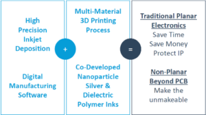
For additive manufacturing to make inroads into the world of electronics requires several ingredients that the traditional additive manufacturing toolset doesn’t include. Resolutions need to be better, multiple materials need to be printed simultaneously in the same machine, and materials must support high temperatures and have specific dielectric properties.
 For additive manufacturing to provide a compelling offering to the electrical engineer it is clear that the approach has to deliver ways to speed up prototyping, bring it inhouse and also open doors to entirely new ways of designing and manufacturing electronics. The same recipe that has brought much success to 3D printing is now in place to do the same to this new electrical domain. Nano Dimension’s DragonFly system is a leading example of the trends bringing together new materials, new designs and new deposition options to deliver a system able to cater to the needs of the market as they currently are, as well as to move the boundaries of what is possible.
Deposition of materials is the key
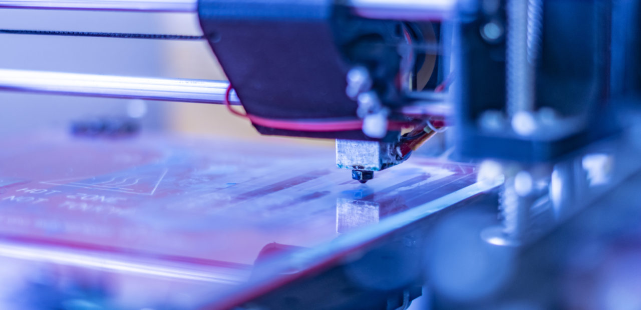
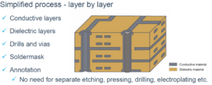
An additive manufacturing approach is clearly based upon the precise deposition of materials. This is a layer-by-layer additive process whereby specific materials are placed in specific locations in order to build up an integrated functional part in a one-system print process.
For an engineer looking to speed up their current R&D cycles, this means bypassing much of the waiting involved in traditional outsourced prototyping. Going from design to functional part in a matter of hours can change how innovators and R&D groups practice their craft. This can get an engineer from PCB design to validated circuit board much more quickly. Given the flexibility of additive manufacturing, the engineer can also consider electrical applications that go beyond traditional PCBs to include designs for antennas, printed capacitance, electromagnets and molded interconnect devices (MIDs).
Rapid progress from design to part
To be clear, additive manufacturing of electronics is not limited to PCBs, it is also used for other types of application development, including devices with new requirements and devices with increasingly complex formats. It’s an ideal fit when faced with geometrical complexity, portability and very small dimensions such as those for semiconductor applications, medical devices, Industry 4.0, the Internet of Things, etc.

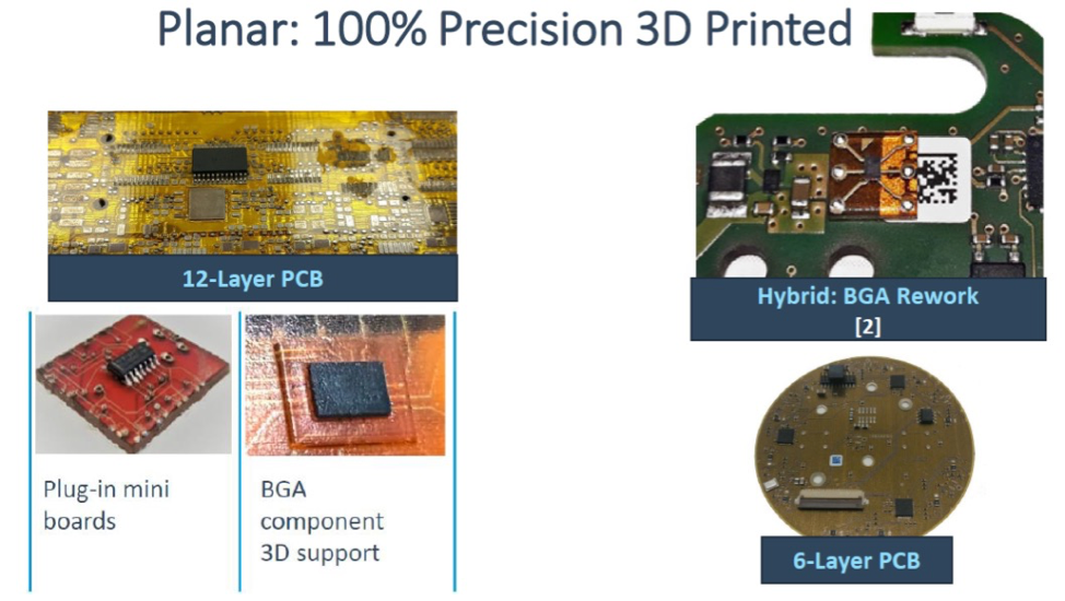
If you are designing a standard planar PCB, then operating a 3D printer such as the DragonFly doesn’t require anything other than your traditional Gerber and Excellon output files. Traditional EDA PCB design packages are focused on meeting the needs of today’s electrical engineers and this means the ability to design circuits and systems of circuits, that are rigid or flexible, planar, multi-layered, high-speed compatible and so on. Designing for the non-planar. All of these can then readily output files that can then be used by the 3D printer.
A new way of thinking
Additive manufacturing is now leading to new ways of thinking about old challenges. Some of these require design tools that can design in the 3rd dimension and designing new capabilities.
-
Capacitors
Additively manufacturing capacitors within the layers of a circuit can create space to meet ever-increasing needs for miniaturization of electronic devices for consumer, industrial, medical and defense applications. With extra space, designers may pack more functionality on the circuit board and shrink component size – all without compromising reliability. -
RF circuits
Working with Harris Corporation, and using the DragonFly to additively manufacture 3D printed RF circuits, the US-based defense contractor found their 3D printed RF amplifier circuits for 6GHz worked as well as those created with traditional methods. -
Side mounting technology
Recently, Nano Dimension announced a world’s first; side mounting technology for additively manufactured PCBs. Using a 3D printer to create a circuit board, components were placed, as is traditionally done, on the top and bottom of the PCB. Components were also added to the sides, resulting in as much as a 50% increase in board space when compared with traditionally manufactured PCBs. 3D printing mounting allowed design engineers to pack more functionality on the circuit board. -
Ball grid arrays
Modern printing technology can shorten and simplify the assembly process for ball grid arrays (BGAs) and other surface mount technology (SMT) components. In a proof-of-concept testing using the DragonFly printer, the time needed to create and populate PCBs with BGAs went from days or weeks to just one hour. Typically, the process from initial design through printing, soldering, manufacturing, assembly, and reflow takes weeks to complete. With a special layout structure that can only be achieved through additively manufactured PCBs, there is no need for special tooling for assembly. This enables in-house manual assembly of BGAs and SMT components during the design and application development phase.
Where are we heading?
Additive manufacturing of electronics, whether circuits, antennas or components is very much a reality. No doubt we are in the early days of the revolution, but 3D printing electronics is here. Developing and deploying increasingly rapid, reliable and material-agnostic printers will only help further the use of this technology. The addition of a broad range of advanced, 3D printable materials and sophisticated electrical design packages capable of truly non-planar electrical design and simulation will see this grow to an everyday part of the electrical engineer’s toolkit.

-
Co-founder of Nano Dimension

A co-founder of Nano Dimension, Simon Fried leads Nano Dimension’s USA activities and marketing for this revolutionary additive technology. With experience working in the US, Israel and throughout Europe, he has held senior and advisory roles in start-ups in the solar power, medical device and marketing sectors. Previously, Simon worked as consultant on projects covering sales, marketing and strategy across the automotive, financial, retail, FMCG, pharmaceutical and telecom industries. He also worked at Oxford University researching investor and consumer risk and decision making.
One Comment
Leave a Reply

- Blog

- Blog
AI in PCB design is increasingly seen as a game-changer, with some predicting it could soon replace entire layout teams—but this view risks overlooking both the current limits of AI and the critical expertise engineering demands. At DesignCon 2025, experts from emphasized that AI's real value lies in complementing human judgment, not replacing it. Read more on our blog.

- Blog
Our new post explores the potential of augmented reality (AR) to transform everyday experiences in shopping, education, and navigation. It highlights how enhanced AR devices will offer immersive, interactive environments that blend the virtual and physical worlds.
- Blog
The field of PCB design continues to evolve as advancements in technology and shifting market demands push the boundaries of what’s possible. By 2025, several key trends are set to shape the industry. Find out more on our blog.
Related Content

- Solutions
Many companies have recently embarked on the “digital transformation” journey to become more efficient and competitive. A recent IDC study showed that 90% of small and medium-size businesses are budgeting for the digital transformation and 73% have begun the process. .

- Products
CR-8000 is a System-Level PCB & IC Package Design software including 3D Multi-board, Analysis and MCAD Integration
Absolutely fascinating read! The evolution of additive manufacturing from mechanical to electronic applications is opening doors we hadn’t imagined a decade ago. The idea of embedding capacitors or side-mounted components through 3D printing is truly a game-changer.
Curious—how close are we to seeing this tech adopted at scale in mainstream consumer electronics manufacturing?