
PCB Design to Manufacture for 3D Printing
Zuken Partners with Nano Dimension to Develop Seamless Design to Manufacture for 3D Printing
5 April 2017 – Westford, MA, USA – Zuken and Nano Dimension are working together to advance the 3D printing user experience and prototype turnaround times. Nano Dimension, a leader in electronic printing technologies, will take advantage of the support for implementing electronic technologies provided by Zuken’s market-leading, native 3D, system-level design solution, CR-8000 Design Force.
We’re excited about working with Zuken to harness Design Force and take our products even further, giving our users a seamless experience from design to output and optimization.
Simon Fried, Chief Business Officer, Nano Dimension, said: “It has been an amazing few years for our company as we’ve fielded interest in our technology. We’re excited about working with Zuken to harness Design Force and take our products even further, giving our users a seamless experience from design to output and optimization.”
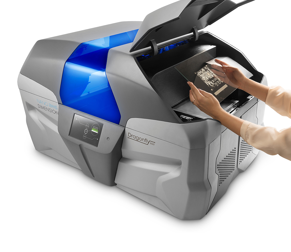
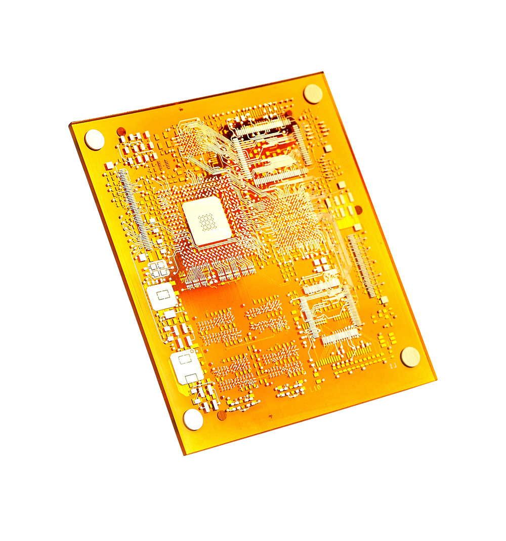
Nano Dimension develops advanced 3D printed electronics platforms, including the DragonFly 2020 3D printer for multilayer printed circuit boards, and nanotechnology-based conductive and dielectric inks for their 3D printers. The printer continues to capture global industry and media attention. Future developments will see expansion to support additional board technologies including flexible circuits and embedded components.
Humair Mandavia, Chief Strategy Officer, Zuken USA, said: “Zuken’s CR-8000 Design Force retains all the detailed data needed for 3D printing and allows export direct to manufacturing or 3D printing, without losing integrity. Nano Dimension’s 3D printers are typical of the many applications we envisioned when we pioneered native 3D design for manufacturing.”
Design Force is the sole design tool that allows specification of unique rules for materials, meaning no extra steps are needed when 3D printing to silver and any other future conductive material. Zuken also offers dedicated DFM solutions to support printed electronics via its DFM Inkjet module that optimizes CAD data for inkjet printers. With these solutions from Nano Dimension and Zuken users can expect to spend more time innovating and getting new ideas to market, rather than dealing with design administration.
DragonFly 2020
Nano Dimension's 3D Printing Platform For Electronics
About Nano Dimension
Nano Dimension Ltd. (NASDAQ, TASE: NNDM), founded in 2012, is focused on the research and development of advanced 3D printed electronics, including a 3D printer for multilayer printed circuit boards, and the development of nanotechnology-based conductive and dielectric inks, which are complementary products for 3D printers. Nano Dimension’s novel and proprietary technologies enable the use of conductive and dielectric inks for ultra-rapid prototyping of complex, high-performance multilayer circuit boards. The company’s PCB 3D printer is the result of combining advanced breakthroughs in inkjet technology, 3D printing and nanotechnology.

- Press Release
May 28, 2026
Valeo and Zuken join forces to redefine automotive electronic design
Valeo and Zuken are partnering through the Zuken Valeo InnoLab to create an open, AI-assisted electronic design platform for automotive engineering. The collaboration combines Zuken’s AI architecture with Valeo’s AI Agents and industrial expertise to reduce design times, strengthen digital continuity, and support robust electronic design across the full design flow.
Read now
- Blog
May 13, 2026
Why PCB Design Has Outgrown Single-Board Thinking
Modern electronic products are no longer built around a single PCB. As systems become faster, denser, and more interconnected, engineering teams are being forced to rethink how they design, verify, and manage complex multi-board products.
Read now
- Technology Partner
- VISIT WEBSITE
April 27, 2026
Marvell Semiconductor
Technology Partner
Marvell Semiconductor provides IBIS (I/O Buffer Information Specification) models for high-speed signal integrity analys...
- Blog
March 25, 2026
Determining Conductor DC-Resistance in CR-8000 Design Force
Explore how CR-8000 enhances PCB design with integrated control of impedance and resistance—enabling precise analysis for both high-speed and high-power applications, from signal integrity to power distribution optimization.
Read now