
3D Printing for Electronic and Electrical Systems
If you’ve tracked some of the hot topics in engineering over the last year, you’re likely very aware of 3D printing or additive manufacturing. This method lays down successive layers of plastic or metallic material that then fuses them together. Over time, those successive layers add up to make fully formed components.
This technology has actually been available in one form or another for a couple of decades. However, advances in the past few years carry some significant implications. Most excitement revolves around the ability to mass produce mechanical parts using this method. For instance, the inherent advantages of additive manufacturing allow engineers to design components with internal voids without concerns for machining or tooling design. Walls can feature lattices of varying density. The next frontier of this technology is controlling the variation of material properties along the length of a part or any other spatial dimension. When these implications become realized, the buzz will be warranted.
How does this relate to electrical and electronic systems design?
The Foundation: Enabling Signals
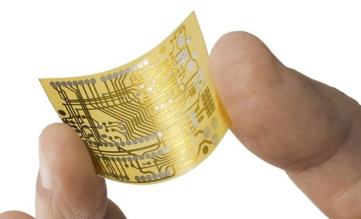
The core innovation that allows the application of 3D printing to electrical and electronic systems design is the ability to print conductive and non-conductive materials side by side, meaning you can have a single layer where a non-conductive material like plastic surrounds a material that carries a signal—like a metal. This mirrors what happens with a trace in a board or a wire in a sheath. Much like a circuit board, the printer can lay down successive layers with different layouts. With 3D printing, you are able to do more than just laying down these traces in a single plane. A trace can go in a direction, come up vertically at an angle to avoid another trace, and continue in another direction.
With this foundation in place, a world of possibilities opens up to apply 3D printing to electrical and electronic systems design.
3D Printing and Electronic Systems Design
Let’s say that you can use 3D printing to make a circuit board. What’s the big deal? Well, there is a range of interesting possibilities.
- The shape of the board could be 3D printed, meaning it would no longer have to be flat. It could be cone-shaped, composed of spirals, and more. Given the space constraints of today’s board systems, this kind of flexibility could be a boon.
- The board and enclosure would consolidate into one part, and they literally could be printed as a single component. This carries some very interesting potential in terms of structural loading and vibration. You could design the single board-enclosure component to avoid certain excitation frequencies.
- Walls of the board, enclosure, or the consolidated board-enclosure could contain latticing. This has a lot of implications for thermal management. Need a new source of airflow? Add in a latticed section to the base, side, or top surfaces.
3D printing applied to electronic systems design means more flexibility. The technology isn’t mature enough for all of these uses yet, but it is on the horizon. Given how constrained board systems have become, many will be pushing firmly towards that future.
3D Printing and Electrical Systems Design
It is fairly straightforward to see how 3D printing applies to electronic systems design, but how does it apply to electrical systems design? The idea is simple: print wires into the structural components of the parts instead of routing them. Instead of running a wire around the internal cavity of a product, you can now PRINT the wire into the external structural parts of the product. Thus, essentially, the internal wires of products go away. What are the implications here?
-
- You can print sensors and their wire connections within structural components. Want to measure strain or temperature in the product? Embed a sensor in a wall with printed wiring.
- You can potentially reduce the weight of products by removing wiring. Embedding it in the structural components or walls of the product, would not eliminate it entirely but would certainly consolidate it.
- Embedding sensors, antennas, and wiring into walls promise to free up space within the internal product cavity. Space-constrained products could realize a significant boon.
All of this assumes that you can 3D print the structural components of the product. Again, the technology is not there quite yet, but engineers are prototyping this technology today. Given the benefits, many companies will be pushing to make this reality sooner than later.
The Takeaway
Additive manufacturing for mechanical components has a ton of buzz right now. Given the benefits, that buzz is warranted. Expect to see some significant progress in the next six months to a year. Many manufacturers of 3D printing equipment are racing to get to production capabilities.
Watch that trend. Pay attention to it. However, don’t sleep on 3D printing for electronic and electrical systems design. Many startups are seriously exploring how to make this real right now. Think about the implications for your design. Think about how your company could realize benefits.
Why?
Because before you know it, this technology will be ready.

-
Chief Analyst and CEO of Lifecycle Insights

- Blog
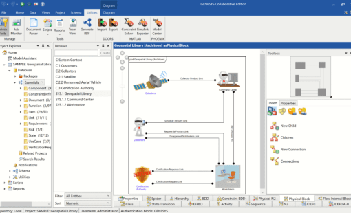
In this week’s blog post we’re sharing an exciting sneak peek of the 2021 R2 release of GENESYS, the latest version of our model-based systems engineering development platform, including a new language option and an extended API.

- Blog
Alex Grove, Account Manager at Zuken, talks about his personal MBSE journey, what his customers experience when embarking on such a journey, and the upcoming Annual Systems Engineering Conference.

- Blog
Digital Transformation should go beyond a simple mapping of analog documents and processes into the digital domain. This blog post explores new ways and opportunities to enhance today’s methods and processes for increased efficiency and accelerated innovation.

- Blog
Many manufacturers are harnessing systems engineering approaches to mitigate the complexity of developing increasingly sophisticated products. Systems simulation is a key component of such efforts.
Related Content

- Solutions
Many companies have recently embarked on the “digital transformation” journey to become more efficient and competitive. A recent IDC study showed that 90% of small and medium-size businesses are budgeting for the digital transformation and 73% have begun the process. .
- Solutions