
Hardware Architecture Design Becomes the Next Competitive Requirement
 After a lengthy quiet period, the hardware design process is suddenly experiencing numerous changes in the form of design discipline convergence and process extension. The widely used 2D single board PCB detailed design process is being replaced by a 3D multi-board and multi-discipline one. What is happening in detailed design is a great blog topic, but I want to talk about what is happening upstream from the detailed design process – hardware architecture design.
What’s the Big Deal About Hardware Architecture Design?
Product complexity is driving the hardware design process evolution. And product complexity is being driven by product miniaturization, IoT, design reuse, security, complex packaging, high density packaging, etc. It’s a long list. The result is that detailed design process is converging into a system-level design abstraction and the overall process is extending upstream into model-based systems engineering (MBSE) and hardware architecture design. The increasing product complexity no longer allows us to leap from requirements to detailed design; we need to better define the system, optimize the hardware system architecture and then move to detailed design.
The need for hardware architecture design and optimization stems from the risk that if you enter detailed design with an architecture flaw (e.g., board won’t route so we need to add a board or enlarge the board, board(s) won’t fit in the enclosure, the product weighs too much) you may not be able to recover. During a recent webinar, one of our polling questions uncovered that fact that 92% of the audience had experienced a PCB fit problem with their enclosure. That’s an architecture failure, not a detailed design failure. In other words, a z-axis collision between a tall component and an enclosure is a detailed design fix, but if changing the shape of the PCB or the enclosure is required to avoid collisions, that is an architecture design failure.
Planning Flow of Hardware Architecture
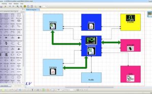
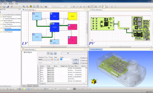
Zuken’s System Planner performs hardware system architecture design and optimization across four disciplines: functional design, PCB planning, space planning and various parametrics that include weight, cost, power, etc. Here is a synopsis of the architecture planning flow:
- System Planner starts with the functional block diagram and that can begin with the schematic of the current version. Most new product designs starts with the current design.
- Add functional blocks from your library or create a block with a partial BOM as a place holder. You can add the schematic later.
- Assign the functional blocks to different PCBs and analyze routability.
- Move functional blocks from board to board to optimize layout and signal integrity.
- Make sure the boards fit in the enclosure and that the parametrics (e.g., cost, weight, power, etc.) meet product requirements. You can also map requirements to functional blocks or boards for traceability.
But Wait, There’s More!
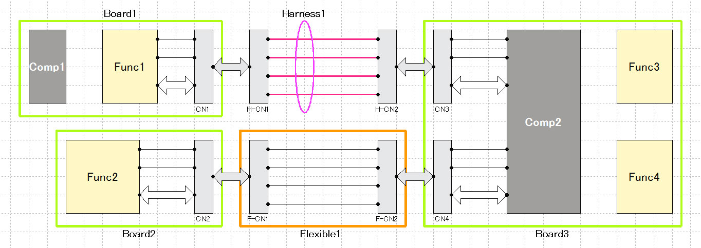
System Planner 2017 has added support for wire harnesses. So now you can design board interconnect in the form of a flex board with a wire harness. More of the discipline convergence I mentioned earlier. Once you have optimized the multi-domain design, the boards move into CR-8000 as a multi-board system. The harnesses move into E3.series for detailed design. No data re-entry required. The integration is seamless.
Hardware system architecture design is becoming a competitive requirement as product complexity is on the rise and the room for error is shrinking. You may not be able to squeeze much more productivity out of your detailed design tools, but you can feed them with higher quality designs. Sound interesting? Check out this page and request a hardware architecture design and optimization demo.

-
Vice President of Marketing, Zuken USA, Inc.

- Blog
Believe it or not, you can use your Circuit Block Library for architectural planning too!

- Blog
Defining initial hardware architecture requires many decisions, most of which impact a variety of different stakeholders and requirements – including multiple design tools – circuit design, PCB layout, mechanical design, spreadsheets, etc. that are used to track different elements of the design.
Related Content

- Products
- Products
System Planner ist das erste Werkzeug, das ein vollständiges Architekturkonzept von Elektronikprodukten unterstützt. Bislang getrennte Schritte werden intelligent in einer einzigen Applikation zusammengeführt.

- Products
CR-8000 umfasst eine Suite von Anwendungen, die den gesamten Lebenszyklus des PCB Engineerings abdecken.