Tech Tip: Creating and Verifying a System Circuit Diagram for Multi-Board Design in CR-8000
Menu
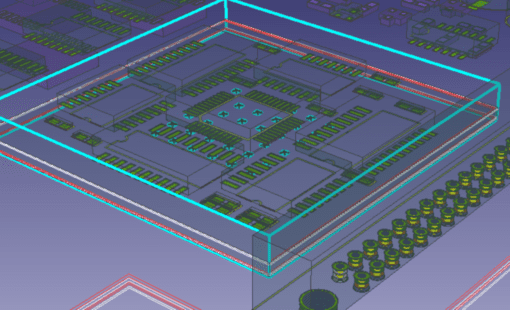
In part 1 of this series, I introduced the different methods for multi-board design in CR-8000. In most cases, the design starts with a system circuit diagram. Today you’ll learn how to create and verify one in CR-8000.
To generate such a system circuit diagram in CR-8000 Design Gateway, a resource file (systemcir.rsc) must be created first, as well as defined how physical connectors are identified. This can be done using the Function Type Number, which is usually found in the CompKind. As soon as the number has been entered into the System Resource File, Design Gateway knows which reference number corresponds to the physical connectors.
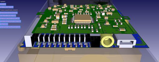
Afterward, the system circuit can easily be created as a new design. All you have to do is check the box for System Circuit in the Design Tree View under the item SDM.
System Circuit Verification
As soon as the system circuit has been created, physical connectors can be extracted from the sub-circuits and linked via System Circuit – Input Board Block. The same principle is used for the second board. Once again, system connectors are placed here.
For the next step, an additional check functionality is available in the Circuit Rule Checker: Physical Connector Mismatch. This feature can be used to check the consistency between placed physical connectors in the design. If the connector in the sub-circuit changes afterward, such a mismatch can be found with this check.
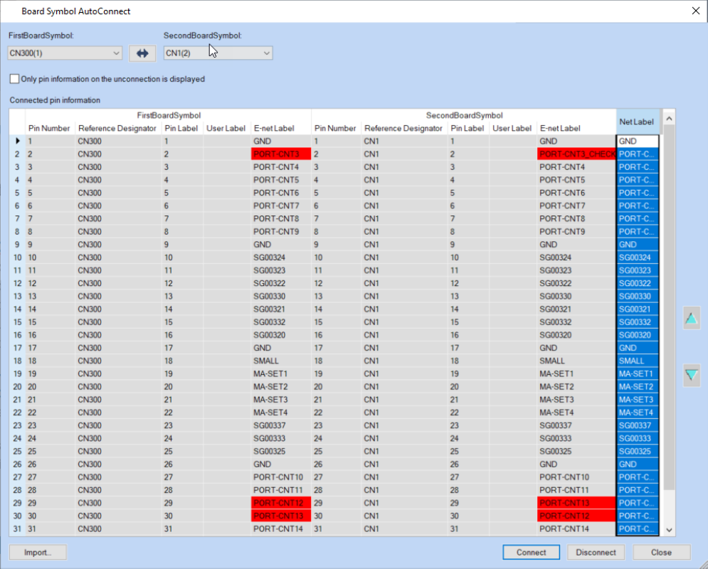
The connectors can be linked manually in the system circuit diagram or with the help of the Board Symbol Auto Connect function. Just select the connectors, start the feature and the connectors will be displayed as a spreadsheet. For each connector the following pin information is listed:
- Pin Number
- Reference Designator
- Pin Label
- E-net Label (New in Design Gateway 2020)
- Net Label
If the suggested connection does not match the developer’s ideas, he can disconnect and reconnect individual lines.
The connectors are then connected to the nets graphically in the design, including a verification of the consistency of the net labels. This check immediately reveals any inconsistencies, for example, due to signal swaps or typing errors. This enables an early verification of the connections between the individual boards in the multi-board design process.
A resource file (autoconnect.rsc) runs in the background for this check. It allows the definition of the column display and the color-coding of the error warnings.
Cross-Probing between designs
Compare Pin Property Utility provides another option for cross-probing between designs. This feature can be used to display the spreadsheet view of the connections between the connectors in the console window with the corresponding pin properties. As before, the system circuit diagram runs through a check that highlights any mismatches in color.

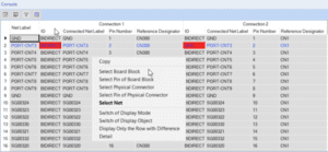
In addition, a right-click with the mouse will enable communication into the system. For example, by selecting Select Board Block or Select Pin, Design Gateway would highlight the system connectors in the system circuit diagram. The same thing applies to Select Pin. Likewise, it would highlight the corresponding pin in the system circuit.
With Select Physical Connector or Select Pin on Physical Connector, the connected system subcircuit diagram will open showing the respective connector with the pin.
These functionalities for multi-board PCB design can be used comfortably as a cockpit to verify a whole system, built up from connected E-nets.
Also see:

- Blog
January 28, 2021
Tech Tip: How to start a Multi-Board Design in CR-8000
Multi-board designs are becoming increasingly important as today's products require higher speeds and more complex circuits in smaller dimensions. There is more than one way to create multi-board layouts in CR-8000.
Read now
- Blog
March 26, 2020
Multi-board design for applications with different voltages
The benefits of developing all boards of a system concurrently on a single CAD canvas. Stacking PCBs, as opposed to connecting with cables, in multi-board design is a current and highly popular trend, as manufacturing costs are reduced and reliability improved.
Read now
- Webinar
October 20, 2018
3D PCB Multi-board Design Basics
Webinar, Design Force
- Products
October 01, 2018
Design Force
CR-8000 Design Force is the fastest, most effective PCB design solution available today. Design Force enables design teams to layout and verify their designs in the context of a complete system or product.
Read now
3D Multi-board PCB Design
- Blog
January 28, 2021
Tech Tip: How to start a Multi-Board Design in CR-8000
Multi-board designs are becoming increasingly important as today's products require higher speeds and more complex circuits in smaller dimensions. There is more than one way to create multi-board layouts in CR-8000.
Read now
- Blog
March 26, 2020
Multi-board design for applications with different voltages
The benefits of developing all boards of a system concurrently on a single CAD canvas. Stacking PCBs, as opposed to connecting with cables, in multi-board design is a current and highly popular trend, as manufacturing costs are reduced and reliability improved.
Read now
- Webinar
October 20, 2018
3D PCB Multi-board Design Basics
Webinar, Design Force
- Products
October 01, 2018
Design Force
CR-8000 Design Force is the fastest, most effective PCB design solution available today. Design Force enables design teams to layout and verify their designs in the context of a complete system or product.
Read now
3D Multi-board PCB Design