
How to Calculate Trace Length for High-speed Signals
Menu
Calculating signal speed on a PCB
According to physics, electromagnetic signals travel in a vacuum or through the air at the same speed as light, which is:
Vc = 3 x 10⁸M/sec = 186,000 miles/second = 11.8 inch/nanosecond
A signal travels on a PCB transmission line at a slower speed, affected by the dielectric constant (Er) of the PCB material. The transmission line structure also affects the signal speed.
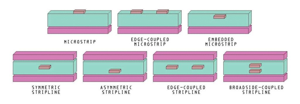
There are two general PCB trace structures [note*]: stripline and microstrip.
The formulas for calculating the signal speed on a PCB are given below:
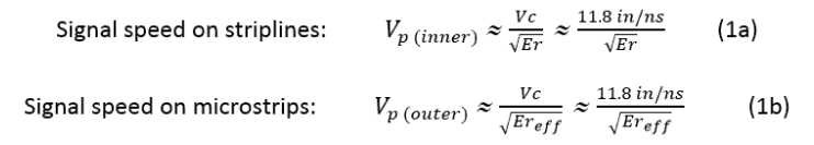
Where:
- Vcis the velocity of light in a vacuum or through the air
- Er is the dielectric constant of the PCB material
- Ereffis the effective dielectric constant for microstrips; its value lies between 1 and Er, and is approximately given by:
Ereff≈(0.64 Er+ 0.36) (1c)
With those formulas, we know that the speed of signals on a PCB is less than the signal speed through the air. If Er≈4 (like for FR4 material types), then the speed of signals on a stripline is half that of the speed through the air, i.e., it is about 6 in/ns.
How to calculate propagation delay (tpd)
The propagation delay is the time a signal takes to propagate over a unit length of the transmission line.
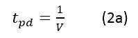
Here is how we can calculate the propagation delay from the trace length and vice versa:
 Where:
- Vis the signal speed in the transmission line
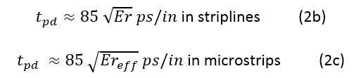
In a vacuum or through the air, it equals 85 picoseconds/inch (ps/in).
On PCB transmission lines, the propagation delay is given by:
Case study: Calculating trace length on a PCB
In order to be compliant with the specification of JEDEC, the maximum skew among all the signals shall be less than +/-2.5% of the clock period driven by the memory controller. All the signals of SDRAM are directly or indirectly referenced to the clock.
In this example, the normal FR4 material with a dielectric constant of 4 is used on the PCB with a differential clock rate of 1.2GHz (i.e., 833ps clock period):
Question: What is the maximum skew of the trace length for all the signals?
Answer: Max skew in time delay = +/-2.5% of the 833ps clock period = 20.825ps FR4 Er≈4, Ereff≈2.92
So, for strip lines, the maximum skew should be less than +/- (20.825/(85*SQT(4))=+/-0.1225 in = +/- 122.5 mil.
For microstrips, the maximum skew should be less than +/- (20.825/(85*SQT(2.92)) = +/-0.1433 in = +/- 143.3 mil.
Note*: Different microstrip and stripline structures will affect the signal speed, but only slightly.
Keep this information in mind the next time you’re calculating trace lengths; it should make the job a little easier for you.
References:
– Signal Speed and Propagation Delay in a PCB Transmission Line, Atar Mittal
– JEDEC
Also see:
CR-8000 – PCB Design Software Overview

Lance Wang is a solutions architect at the Zuken SOZO Center. He supports the CR-8000 product line, mainly focusing on high-speed PCB design and signal integrity features. When not behind the keyboard or in front of customers, he is a Tom Brady fan and enjoys playing ping pong in his spare time.

- Blog
May 23, 2025
AI in PCB Design: From Misconception to Meaningful Assistance
AI in PCB design is increasingly seen as a game-changer, with some predicting it could soon replace entire layout teams—but this view risks overlooking both the current limits of AI and the critical expertise engineering demands. At DesignCon 2025, experts from emphasized that AI's real value lies in complementing human judgment, not replacing it. Read more on our blog.
Read now

- Blog
February 13, 2025
The Future of Augmented Reality
Our new post explores the potential of augmented reality (AR) to transform everyday experiences in shopping, education, and navigation. It highlights how enhanced AR devices will offer immersive, interactive environments that blend the virtual and physical worlds.
Read now

- Blog
January 30, 2025
The Top PCB Design Trends to Watch in 2025
The field of PCB design continues to evolve as advancements in technology and shifting market demands push the boundaries of what’s possible. By 2025, several key trends are set to shape the industry. Find out more on our blog.
Read now

- Blog
January 23, 2025
Supply Chain Risk Management in PCB Design with SiliconExpert and CR-8000 Integration
Supply chain risk management is critical for electronics design. By integrating SiliconExpert with CR-8000, engineers gain tools to streamline component selection, manage obsolescence, and ensure design continuity. This integration supports efficient workflows, reduces costs, and mitigates supply chain disruptions.
Read now
Related Content

- Webinar
November 15, 2019
How to be First to Market with DDR5!
DDR5 is the latest generation of memory. In this joint webinar with Keysight Technologies, we’ll begin with pre-layout simulation, then transition to CR-8000. The design will then be verified by Electromagnetic (EM) simulation and system simulations in Keysight ADS, in order to build confidence in the final DDR5 design.
WATCH NOW
- Products
January 03, 2019
Simulation and Analysis
CR-8000 includes fully-integrated simulation and analysis tools to verify all aspects of your single or multi-board designs
Read now
Integrated simulation and analysis tools