Automated creation and modification of pin assignments of complex circuits in PCB designs
Commissioned by Bosch Car Multimedia, Zuken’s Custom Development Group has developed a solution that enables simultaneous IC, connector, and PCB development by automating the updating of pin assignments in the PCB design. The solution reads pin assignment lists of SoC modules or connectors with high pin counts into CR-8000 Design Gateway and automatically creates connections, busses, and hierarchy links in IC devices in the schematic. This enables a significant reduction of effort and the risk of errors in the update of PCB designs.
Tight innovation cycles in the field of automotive electronics require a close synchronization of the development processes of control units, connectors, and PCBs. Since the pin assignment of control units and connectors is subject to frequent changes with the growing functionality, it is necessary to update the pin assignment of the affected elements on the PCB side on a regular basis.
Automating this update as much as possible and avoiding manual – and thus inherently error-prone – changes to the PCB design as much as possible was the objective of an add-on software program that Zuken developed on behalf of Robert Bosch Car Multimedia GmbH, Hildesheim. The solution, called Automatic Block Update, has recently been successfully put into productive operation.
Automatic Block Update (ABU)
The functionality of Automatic Block Update can be described as follows: Pin assignment lists (referred to as PAL or Pin Assignment List in the illustration below), which are provided by IC development in a machine-readable format, are read into Zuken’s CR-8000 circuit development environment Design Gateway via Automatic Block Update and automatically updated (Figure 1).
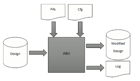
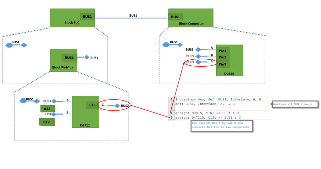
The Automatic Block Update automatically generates all required connections, bus connections, and hierarchical connectors that provide connectivity between the sheets of hierarchical designs. The changes are automatically generated in multiple passes on all sheets and levels of Design Gateway. (Fig. 1)
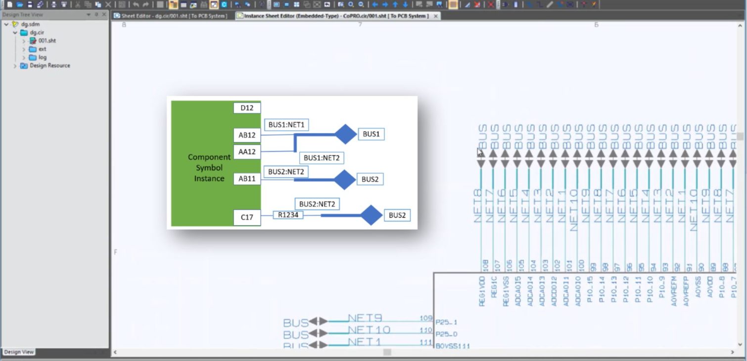
Creation of net connections, bus connections, and sheet connectors
For every unconnected pin in the IC device within Design Gateway (shown as a green rectangle in the graphic), the required connections are created in an automated process (Fig. 2):
- The net connection (thin blue line)
- a bus connector (thick blue line)
- and a sheet connector (blue rhomb)
- In addition, a hierarchy connector is created on the same sheet where the IC symbol is placed. This is used to connect the bus concerned to the next higher level (Fig. 3).
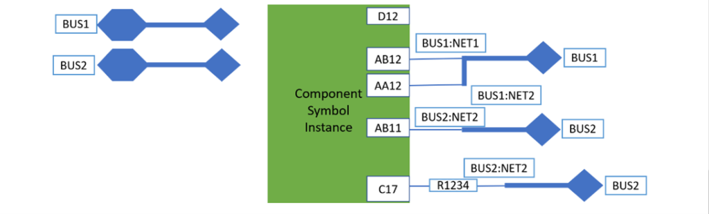
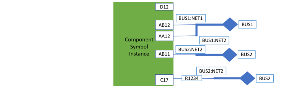
If a wire with a passive component is already connected, and a Net Bus Connector Group has already been created behind it, these existing nets and bus connections will be updated automatically via the Automatic Block Update. Nets that were already connected, will be renamed automatically.
All changes made to the schematic in the course of the block update are documented in a log file and can be reset to the initial state by means of an undo function, if necessary. The function can be started either for the entire design or for a selected block.
ABU enables a clear advantage for pin assignments
“The introduction of ABU has enabled a significant reduction of PCB development time at Bosch Car Multimedia,” says Klaus von Treufels, Technical Director of HW Architecture and System Design. “At the same time, ABU prevents circuit diagram errors that inevitably occur in manually created circuit diagrams.
With the automatic processing using ABU, the entire process took 5:17 minutes, whereby 1:58 minutes were spent on reading in the circuit diagram and 3:19 minutes on writing the result of the update back into the circuit diagram. The actual computing process was completed in less than one second.
When the same task was performed manually by an experienced operator, who was able to carry out all the steps without thinking, it took 7:50 minutes. The time required for an automatic verification run (design rule check), which has to be carried out to exclude errors during manual pin assignment, was not included in this calculation. In the specific example, another 1:15 minutes were needed to carry out the design rule check, plus another 3:00 minutes to get familiar with the circuit diagram.
A significant reduction in PCB development time
Even for very a simple use case, the result is clearly in favour of ABU, even if the design rule check is not taken into account, which is absolutely necessary if the circuit diagram is edited manually.
For more complex use cases, the duration of the Automatic Block Update will remain fairly constant, whereas the duration of manual schematic editing will increase in a more than linear way.
It should be noted that the time taken to read in and write back the new connections depends essentially on the size of the circuit diagram, and not on the number of changes in the actual block update.
New Live Webinar
If you are interested in seeing the functionality of the Automatic Block Update for CR-8000, don’t miss our webinar on October 21st. Marcel Voges, Customer Support Engineer, will be happy to show details and answer your questions.

- Blog
Modern electronic products are no longer built around a single PCB. As systems become faster, denser, and more interconnected, engineering teams are being forced to rethink how they design, verify, and manage complex multi-board products.
- Blog
Explore how CR-8000 enhances PCB design with integrated control of impedance and resistance—enabling precise analysis for both high-speed and high-power applications, from signal integrity to power distribution optimization.

- Blog

- Blog
AI in PCB design is increasingly seen as a game-changer, with some predicting it could soon replace entire layout teams—but this view risks overlooking both the current limits of AI and the critical expertise engineering demands. At DesignCon 2025, experts from emphasized that AI's real value lies in complementing human judgment, not replacing it. Read more on our blog.