Multi-board constraint browser to view and analyze system level interconnects.
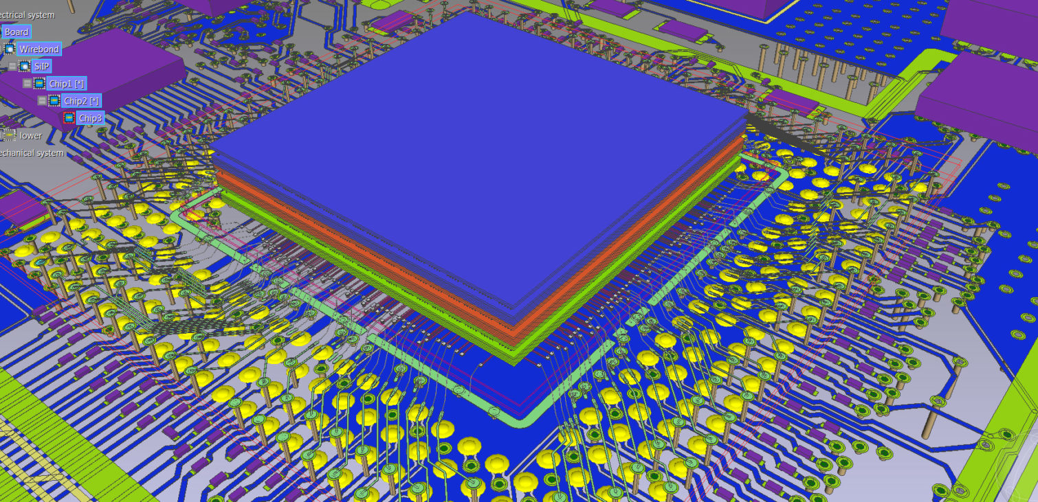
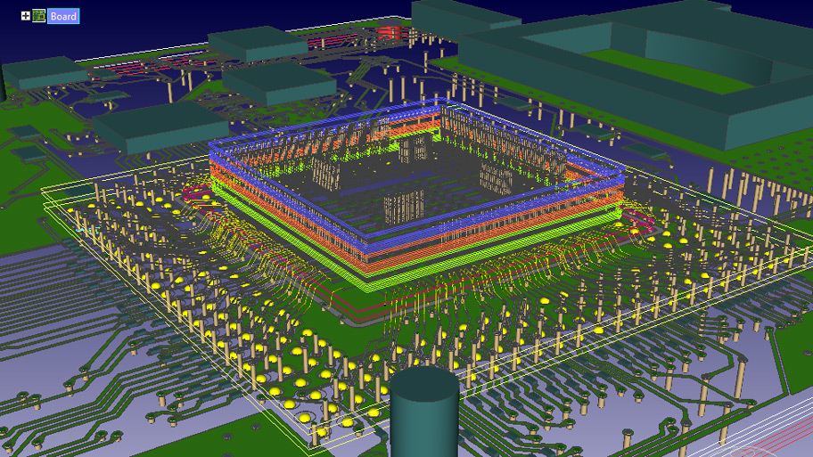
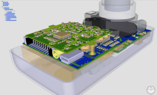
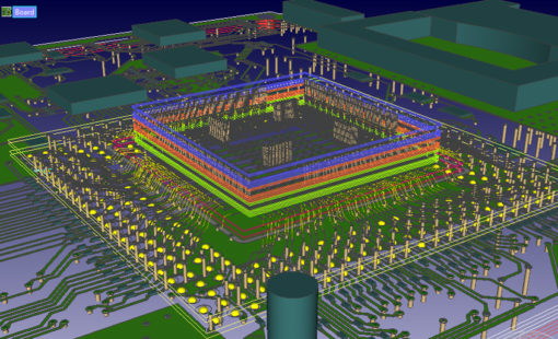
In addition to advanced PCB layout capabilities, Design Force provides chip, package and board co-design capabilities to enable real time 3D hierarchical design. This allows design teams to concurrently create any combination of advanced stack dies, packages and PCBs.
Multi-board constraint browser to view and analyze system level interconnects.

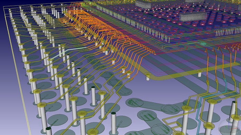
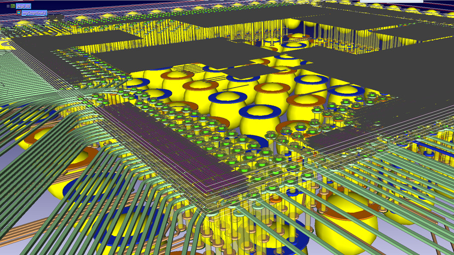
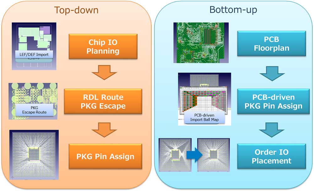
Automatic ball assignment with the ability to optimize complex routing solutions

Single environment for high-speed design with constraint management and SI and PI analysis

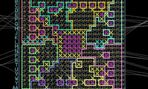
Powerful routing engines for rapid feasibility studies or detailed RDL and bump escape routing of signals and power and ground nets
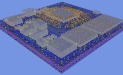
Comprehensive system co-design recognizes the interaction between chip, package, and board data to reduce complexity, size and cost of the overall system.
Design Force chip, package and board co-design provides a technology-rich and device-rich design environment for implementing traditional and advanced node design structures like die + package + PCB, SiP, PiP, and interposer + TSV.
Design Force Chip-Package-Board Co-Design provides a single environment solution for maximum system optimization.
Design Force supports integrations to best-in-class tools from partners such as ANSYS, AWR, Agilent and Synopsys for RF, Full Wave FD/TD, power integrity, and thermal extraction and analysis. This allows designers to address key issues early in the design process.
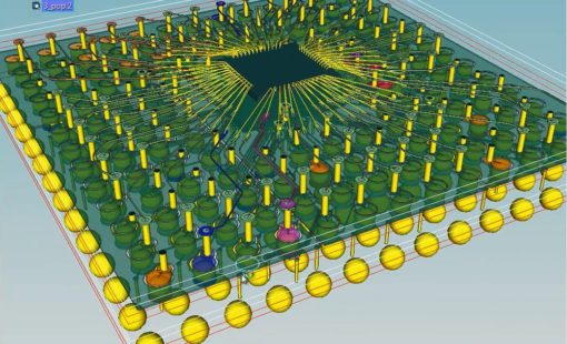
Design Force offers an intuitive, integrated environment for designing single and multi-die packages for wire-bond, flip-chip, and high density advanced packaging. Designers can start designs with early prototype input of chip and package data from the library, reuse data from IC layout tools, and take advantage of parametric wizards to streamline the creation of the system
Design Force combines traditional 2D design with native 3D design and the latest human interface techniques, accelerated graphics and almost instantaneous rendering and refreshing. It is the fastest, most effective PCB design solution available today. Design Force enables design teams to layout their designs in the context of a complete system or product.
The following can be added to extend the functionality of Design Force
Post layout extraction of single and coupled (crosstalk) routed traces; What-if analysis; Cross-section view for traces.
A simulation environment for post layout signal integrity simulation.
A powerful PCB-FPGA co-design environment that enables exchange of I/O and constraint information between PCB designs and FPGA designs.
A simulation environment for Power Integrity (AC impedance and de-coupling impact, DC voltage drop, current analysis) and electro-magnetic interference (EMI full board screening, differential mode, common mode, power bus noise).
Fast and easy check of the current density of a layout structure towards a given maximum.
Find out more about CR-8000 Design Force Chip-package-board-co-design via our webinars, blogs, press releases and more...