
Tech Tip: PCB Net Visualization with CR-8000’s Main Path View
PCB designers often spend months on a board, placing components in the perfect spot. While many PCB tools can automatically place and route components, advanced PCB software offers additional analysis and features to help designers place components in optimal locations. CR-8000’s PCB net visualization, using the Main Path View feature, shows only what the designer needs for placement.
Net distance determines component placement
PCB component placement is not an exact science. Connectors, processors, memory devices, power ICs, or other key components may fit in many locations, but the best placement depends on many factors. Designers consider board shape, mechanical keepout zones, thermal constraints, routing paths, and much more.
Net distance plays a major role in component placement. The further apart the related components are placed, the longer the routed path connecting them. It’s not just cluttering the board; longer routes have technical consequences:
- In high-speed signals, long routes affect timing and impedance, which can lead to signal loss and noisy signals.
- In power nets, long paths increase voltage drop and heat
PCB designers need connectivity data before they place components to minimize routing paths.
PCB net visualization gets crowded
Most PCB design tools can show nets, but seeing every connection at once is not always helpful. In a dense design, unconnected nets can quickly become a web of overlapping lines. The information is hard to interpret.
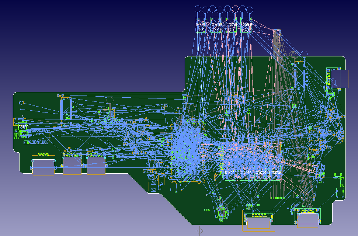
The problem is especially noticeable around ICs, connectors, and power networks. These components often connect to many signals, planes, devices, and supporting circuitry. When too many nets are displayed at the same time, the designer may spend more time filtering the view than understanding the design.
The goal isn’t to see every net, but to only visualize the critical nets that need to be minimized in component placement.
PCB net visualization in CR-8000 with Main Path View
CR-8000 Design Force 2026 introduced the Main Path View feature to help designers see the path of signal and power nets between major components. Instead of relying on a crowded web of numerous nets, designers can use Main Path View to focus on key paths between key components.
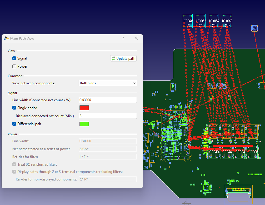
This gives PCB designers a clearer view of the connections that matter most during layout planning. Main Path View helps separate important signal and power paths from the surrounding net clutter, making it easier to understand how major components relate to each other across the board.
Main Path View gives designers control over how main signal and power paths are reviewed. Users can…
- Switch between signal and power nets to focus on the type of connection being evaluated.
- View paths from the A-side, B-side, or both sides of the board to understand how selected components connect across the layout before they are moved into position.
- Change the tag settings used to define main path targets so teams can decide which components are treated as “main” components based on their design process or the situation being reviewed.]
Tips and Tricks for using Main Path View
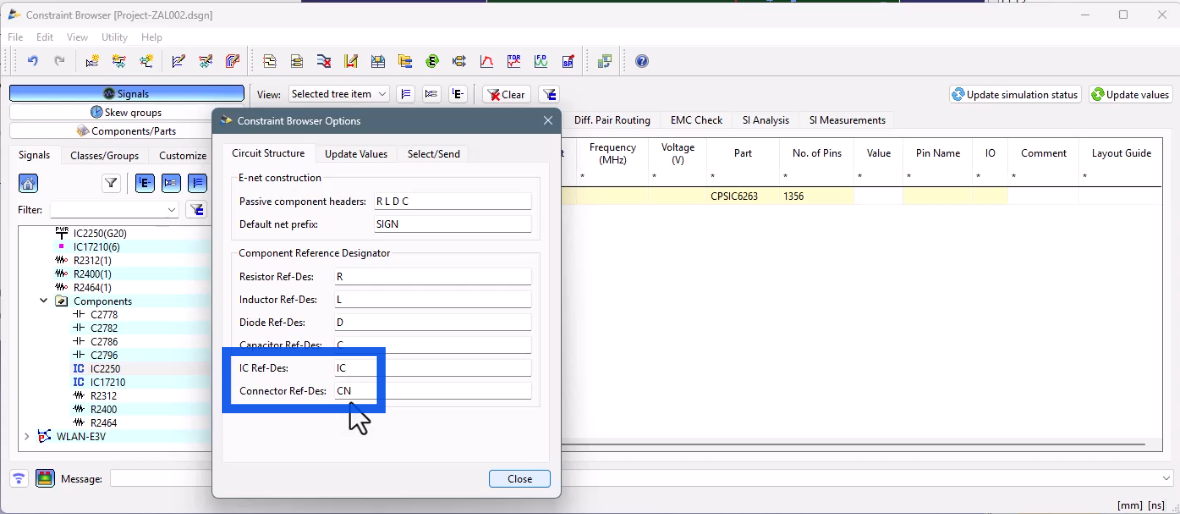
1. Customize reference designator tags to your naming convention
Main Path View identifies “main” components with reference designator tags. By default, ICs are recognized by the prefix “IC” and connectors with the prefix “CN”, but this can be configured in the Constraint Browser.
2. Understand graphical differences in the highlight line
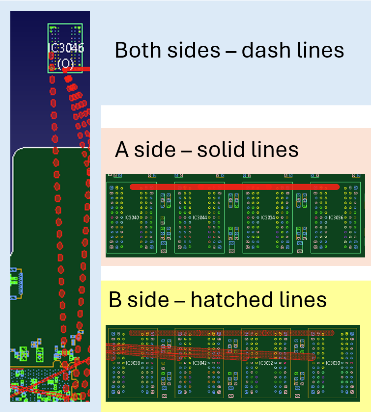
The tool highlights connections between ICs and connectors as Main Paths. Line styles show whether each path is on the A-side, B-side, or both.
- Dotted lines: Connections between A-side and B-side components.
- Solid lines: Connections between A-side components only.
- Hatched lines: Connections between B-side components only.
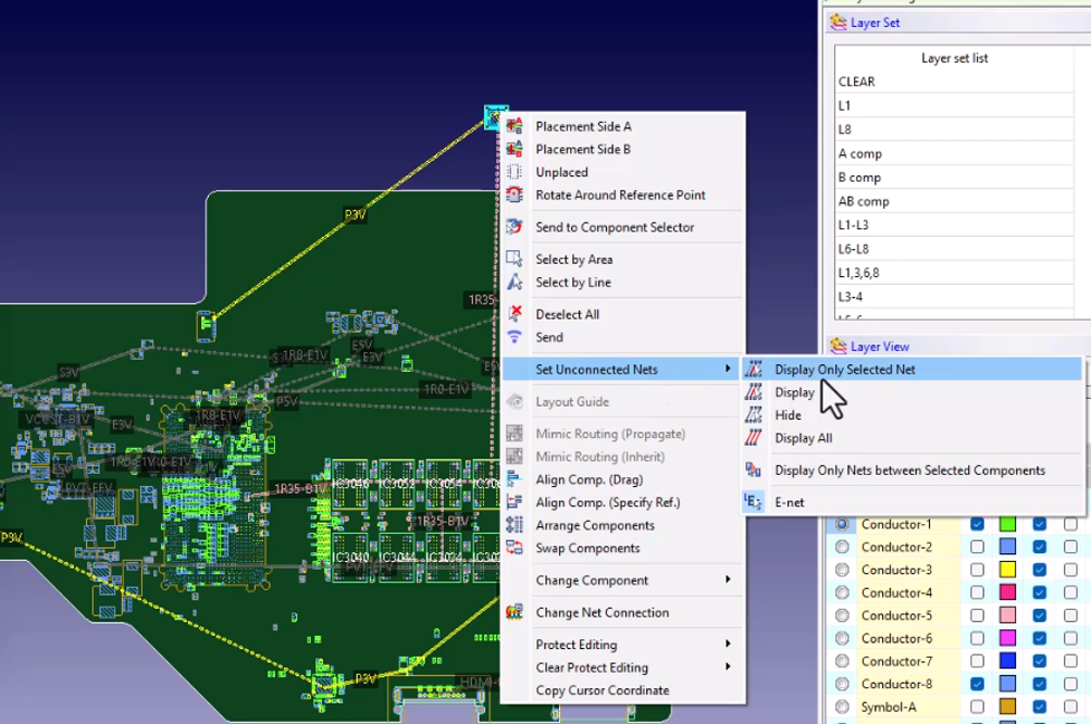
3. Only display the nets of the selected device
The Display Only Selected Net button hides other power nets and shows only the net connected to the selected IC component. This helps reduce visual clutter so designers can focus on the power paths of the device they are placing.
Watch our Video
Who Uses PCB Net Visualization
PCB layout designers use the Main Path View to see how major ICs and connectors are connected as they refine component placement and route planning. This helps them consider the length of critical nets before detailed routing begins.
Design reviewers and team leads use Main Path View to quickly understand high-level connectivity during layout reviews. Instead of a crowded view of all nets, reviewers can focus on the main paths that affect layout decisions.
Next Steps: Strengthen Your PCB Design with CR-8000
PCB net visualization is a critical aid for component placement. By highlighting main paths, CR-8000 helps PCB designers filter through visual clutter and identify better locations for ICs, connectors, and other key components.
Main Path View is one of many Design Force capabilities that help teams design complex PCBs. From constraint-driven design and advanced routing tools to thermal analysis and manufacturability checks, CR-8000 helps engineering teams make layout decisions with a deeper understanding of how each choice affects the final PCB.
To learn more about PCB design with CR-8000:
- Visit the CR-8000 product page
- Read more PCB layout validation tech tips
- Watch this webinar on signal and power integrity in high speed designs

-
Applications Engineer

- Blog

- Blog
- Blog
- Blog
Related Products and Resources
- Blog
- Blog
- Blog
- Blog