
Phased Array PCB Design: Beamforming and Engineering Considerations
Phased arrays steer antenna beams without mechanical movement. Instead, many small antenna elements work together to control the beam’s direction and shape. Their speed, precision, and compact form support advanced radar and communications systems.
However, engineering a phased array introduces significant complexity. Electronics engineers must manage repeated RF channels, precise signal behavior, power delivery, thermal conditions, and thousands of components and connections.
Successful phased array PCB design depends on maintaining consistent electrical performance across the entire array. This post explains how phased arrays work and examines the PCB design challenges they present.
What is a Phased Array?
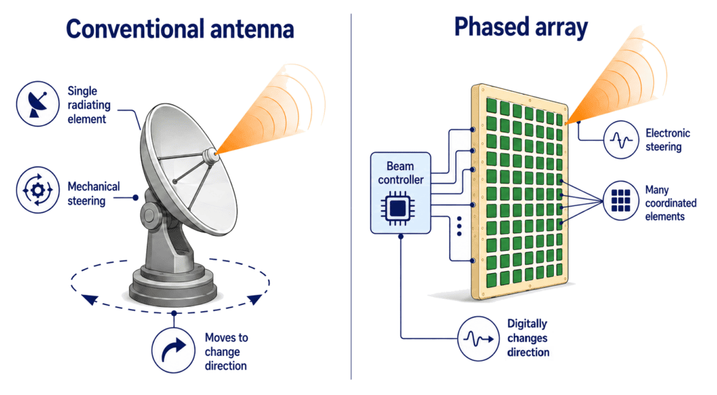
Antennas transmit and receive radio waves for communication, navigation, sensing, and detection. A mechanically steered antenna changes direction by physically rotating the antenna or its reflector.
A phased array takes a different approach. It combines many small antenna elements that work together to form a strong, directional beam.
By changing the phase of the signal at each element, the array antenna steers the beam electronically. No rotating structure is required. As a result, the antenna can respond quickly, track moving objects, and direct energy away from unwanted areas.
Its flatter, more compact design also suits applications where large, moving antennas are impractical. These advantages make phased arrays valuable for radar, satellite communications, 5G networks, automotive sensing, weather monitoring, aviation, defense, and radio astronomy.
Although their size and structure vary by application, all phased arrays rely on precise coordination among their antenna elements.
How Phased Arrays Steer a Beam
Each array element is a small, simple antenna that radiates over a broad area. Supporting circuitry controls the signal transmitted or received by each element. When neighboring elements transmit at the same phase and amplitude, their waves reinforce in one direction. This creates a beam that points straight ahead.
Introducing a controlled phase offset shifts where the waves reinforce. The strongest combined signal then forms at an angle, steering the beam in a new direction.
Some wideband systems use true-time-delay techniques rather than fixed-phase shifts. Both methods control the relative signals across the array, but they behave differently over wide frequency ranges.
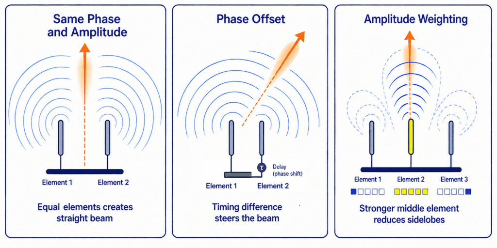
The controller may also adjust the amplitude, or the signal strength applied to each element. This amplitude weighting helps control beamwidth and reduce unwanted sidelobes. However, it may also reduce the array’s peak gain.
Several other factors affect beam performance:
- Element spacing: Spacing influences how signals combine and whether unwanted grating lobes form.
- Array size: A larger aperture generally supports a narrower beam and higher directivity.
- Operating frequency: Frequency affects wavelength, element dimensions, spacing, and transmission loss.
Coordinating these factors becomes increasingly complex as arrays grow larger and operate across wider frequency ranges.
Electronics Design in Phased Arrays
A phased array antenna may contain dozens, if not hundreds, of similar antenna elements. Each element includes components and circuitry that transmit, receive, and adjust its portion of the signal.
Typical channel components include:
- Radiating element: Transmits and receives radio waves.
- Feed network: Carries RF signals between the antenna element and beamforming electronics.
- Beamforming electronics: Phase shifters control phase, amplifiers adjust signal strength, and switches manage transmit and receive modes.
Array-level electronics coordinate the behavior of these individual elements. A beam controller calculates phase and amplitude settings, synchronizes timing, manages transmit and receive switching, and applies calibration data.
Clocking, control buses, power regulation, and RF distribution networks must reach every channel without introducing excessive noise, loss, or variation.
Key Phased Array PCB Design Challenges
Repeated circuits make phased array PCB design especially demanding. Small differences between channels can affect the direction, shape, and strength of the beam. Engineers must manage several connected design factors.
Controlled Impedance and Electrical Length
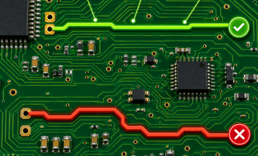
RF traces must maintain controlled impedance and consistent electrical length. Geometrically identical traces may still behave differently if they use different layers, vias, reference planes, or dielectric materials.
Stackup and Material Selection
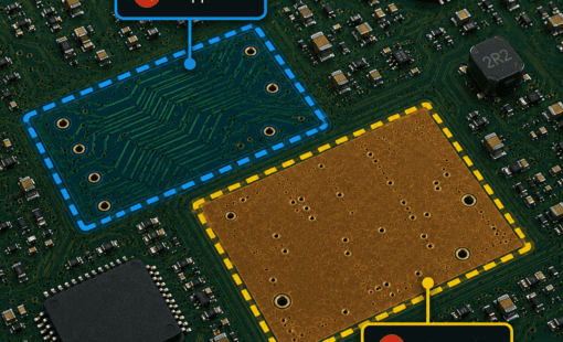
Laminate properties affect insertion loss, phase stability, and signal propagation. Engineers must consider dielectric constant, loss tangent, copper roughness, layer thickness, and surface finish.
Repeated-Channel Consistency
Similar RF channels should use consistent placement, routing, via transitions, and reference-plane structures. Manual duplication increases the risk of small differences that are difficult to identify later.
Power and Thermal Management
Amplifiers and transmit/receive modules can draw substantial current and generate concentrated heat. Voltage drop and temperature variation may change gain and phase across the array.
Manufacturing tolerances also affect channel behavior. Therefore, many arrays require calibration even when the PCB layout appears consistent.
How CR-8000 Supports Phased Array PCB Design
Phased arrays often repeat similar RF channels dozens, hundreds, or even thousands of times across a PCB. Maintaining those channels manually becomes difficult as engineers change components, routing, constraints, and power distribution.
CR-8000 helps teams reuse design data and maintain alignment between the schematic and PCB layout. Reusable circuitry can reduce manual duplication, while design constraints help engineers apply routing, spacing, and connectivity requirements more consistently.
This consistency is important in phased array PCB design. Differences in trace topology, via count, component placement, or reference-plane transitions can change insertion loss and electrical phase.
CR-8000 also helps teams manage design changes across large, component-dense boards. Keeping logical and physical design information connected makes it easier to identify affected circuits, coordinate revisions, and reduce inconsistencies between repeated channels.
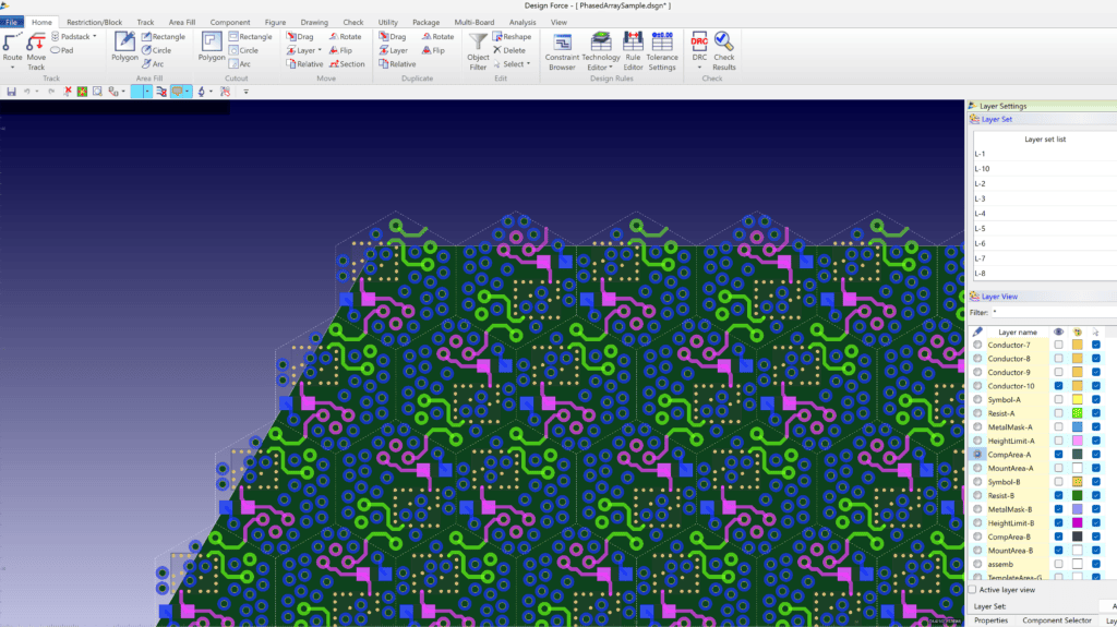
To ensure data consistency and minimize editing time, CR-8000 lets engineers create one or more antenna modules linked to a definition circuit. When the definition circuit changes, engineers can propagate those updates to many or all instances placed on the PCB. Individual instances can also be modified separately when needed. If required, they can later be realigned with the definition circuit. Engineers remain in control of how and when updates are applied. This methodology makes it possible to update repeated circuitry quickly across the entire design without manually editing each instance.
Engineers may still use specialized electromagnetic simulation tools to analyze antenna structures and RF behavior. CR-8000 provides the PCB design environment needed to coordinate circuit intent, layout implementation, constraints, and engineering changes.
Improve Control of Complex Phased Array PCB Designs
Phased arrays combine antenna theory, RF electronics, power delivery, thermal management, and detailed PCB implementation. As element counts increase, maintaining consistent design data becomes increasingly important alongside the design of each individual channel.
CR-8000 helps engineering teams manage repeated circuitry, design constraints, and schematic-to-layout changes within a connected PCB design process.
Learn more about CR-8000 and its capabilities for complex PCB design.

-
Manager of Engineering Operations, SOZO Center at Zuken USA Inc.

- Blog
- Blog
- Blog

- Blog
Related Products and Resources
- Blog

- Blog
- Blog
- Blog