
Why System-Level PCB Design Matters for Multi-Board Products
A printed circuit board can pass every board-level check and still create problems when it reaches the final product.
The PCB may not fit comfortably inside its enclosure. A connector may be hard to reach. Components may conflict with another assembly. A power, signal, or mechanical decision made for one PCB may create a new constraint for another.
These are not always PCB layout errors. Often, they are system-planning issues that remain hidden until detailed design is already underway.
Modern PCB development must move beyond treating each board as an independent design. Decisions about partitioning, connectivity, enclosure fit, and verification often affect several boards at once.
System-level PCB design addresses these relationships earlier, giving engineers a clearer understanding of the complete electronic subsystem before detailed implementation begins.
Advanced PCB design software, including CR-8000, supports this process through functional partitioning, interconnection planning, physical evaluation, early verification, and implementation on connected PCBs.
Why Single-Board Design Falls Short in Complex Electronic Systems
Traditional PCB development often begins after the boundaries of the board have already been established. Engineers receive requirements, create the schematic, define the board, place components, route connections, and verify the result.
That process works when the board’s role is clear, and its relationships with the rest of the product are stable.
However, many modern products contain several interconnected PCBs. These boards may share power, high-speed signals, communication links, cooling requirements, or mechanical interfaces. The design of one board can directly affect the size, placement, connectivity, or performance of another.
A locally optimized PCB may therefore be a poor fit for the subsystem as a whole.
When teams plan boards independently, they often coordinate changes through separate files, spreadsheets, meetings, and manual updates. Each board may remain technically correct on its own, yet the complete product becomes harder to integrate.
PCB leads and electronics architects need a broader view. They must understand not only whether each board works, but also how the boards work together.
Define the Electronic Architecture Before Detailed PCB Design
System-level planning does not mean completing the entire design before schematic capture begins. Instead, it means defining enough of the electronic architecture to guide detailed development.
Before individual PCBs move into implementation, teams should answer several important questions:
- What major functions must the product perform?
- How should those functions be divided across the boards?
- How will the boards connect and exchange power or information?
- Do component cost, availability, or other bill of materials (BOM) constraints affect the proposed architecture?
- What enclosure, connector, signal, or physical constraints could influence the architecture?
- What assumptions need to be validated before detailed design begins?
These decisions establish the structure of the electronic subsystem.
Making them early gives the team more flexibility. Engineers can move functions between boards, reconsider interfaces, or adjust preliminary board definitions without disrupting detailed circuitry and layout work.
The goal is not to freeze the architecture too soon. Rather, it is to identify and evaluate the decisions that will shape the PCBs while changes are still manageable.
How System-Level PCB Design Improves Multi-Board Planning
Multi-board planning gives engineers a shared view of the subsystem’s functions, boards, and connections.
Instead of treating each PCB as an independent project, teams can examine how responsibilities are divided and how the boards interact. This is especially useful during functional partitioning.
A function may fit logically on one PCB but create an impractical connection scheme. Combining functions may simplify interfaces but make a board larger or more complex. Separating them may support reuse or modularity, but it can increase the number of inter-board connections.
Consider a hypothetical design in which the communications function is assigned to the main control board. During mechanical planning, the team finds that the required connector location creates an enclosure conflict. Moving the function to a second board resolves the fit issue. However, it also changes the inter-board connections, connector count, signal path, power distribution, and verification needs.
When the boards are developed independently, each group may discover different consequences at different times. With a shared multi-board plan, the team can compare both arrangements before detailed design work begins on either option.
That broader view also improves communication. PCB designers, electronics architects, mechanical engineers, and project leads can work from the same proposed system structure.
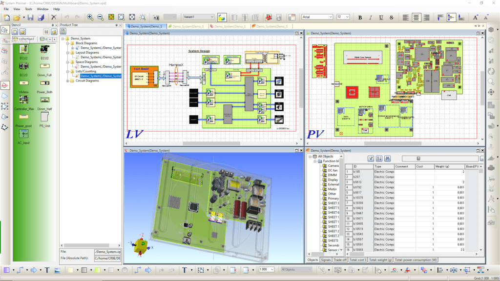
CR-8000 System Planner supports this early stage of development. Teams can define the logical architecture, partition functions across single or multiple PCBs, and evaluate the proposed system before detailed design begins.
The value extends beyond a higher-level diagram. Engineers can establish useful design context and evaluate trade-offs before committing significant effort to individual boards.
Evaluate Mechanical Constraints and System-Level Performance Earlier
A PCB is both an electrical design and a physical object.
Its dimensions, orientation, connector locations, and position within the product can influence the electronic architecture. These factors become especially important when several boards must fit and connect within one enclosure.
When the mechanical context enters too late, teams may discover that an electrically valid design is difficult to integrate physically. Late changes to board dimensions, placement, or connectors can also affect other engineering decisions.
By incorporating mechanical CAD (MCAD) and enclosure data into system planning, teams can assess preliminary board definitions within the product’s physical environment.
The mechanical design does not need to be complete. It only needs enough maturity to answer useful questions:
- Do the proposed boards fit within the enclosure?
- Can engineers position and connect them as intended?
- Are important interfaces accessible?
- Are there obvious clearance or interference concerns?
- Does the proposed functional partitioning make sense within the available space?
CR-8000 System Planner can represent single- and multi-board systems in 3D and place them within enclosure data for early fit and clearance evaluation.
Verify System Assumptions Before Detailed Implementation
Mechanical fit is only one part of early system evaluation.
An architecture may look reasonable but still contain assumptions that need to be tested. System-level verification helps teams identify potential problems before detailed PCB design is complete.
For example, engineers may need to confirm the completeness and consistency of connections, review board-to-board interfaces, or evaluate preliminary board definitions against physical constraints.
Early topology and constraint planning can also provide a stronger foundation for later signal integrity, power integrity, and electromagnetic compatibility analysis.
However, early verification does not replace detailed PCB analysis or final design checks. It addresses a different question.
Detailed verification asks whether the implemented PCB meets its requirements. Early system-level verification asks whether the proposed architecture provides all boards with a realistic path to meeting those requirements.
That distinction matters. Revising a functional partition during planning is less disruptive than redesigning several boards after their schematics and layouts have advanced.
CR-8000 System Planner brings functional partitioning, PCB planning, mechanical context, and parametric evaluation together at the architecture stage. This helps teams evaluate system assumptions as soon as the available data makes those checks useful.
Connect System-Level Planning to Detailed PCB Implementation
Early planning creates limited value when teams must recreate its results downstream.
Manual handoffs can introduce gaps between the proposed architecture and the implemented design. Board definitions may be interpreted differently, connectivity may be entered incorrectly, or changes may not carry consistently between design environments.
A connected workflow reduces these risks by carrying planning information into detailed design.
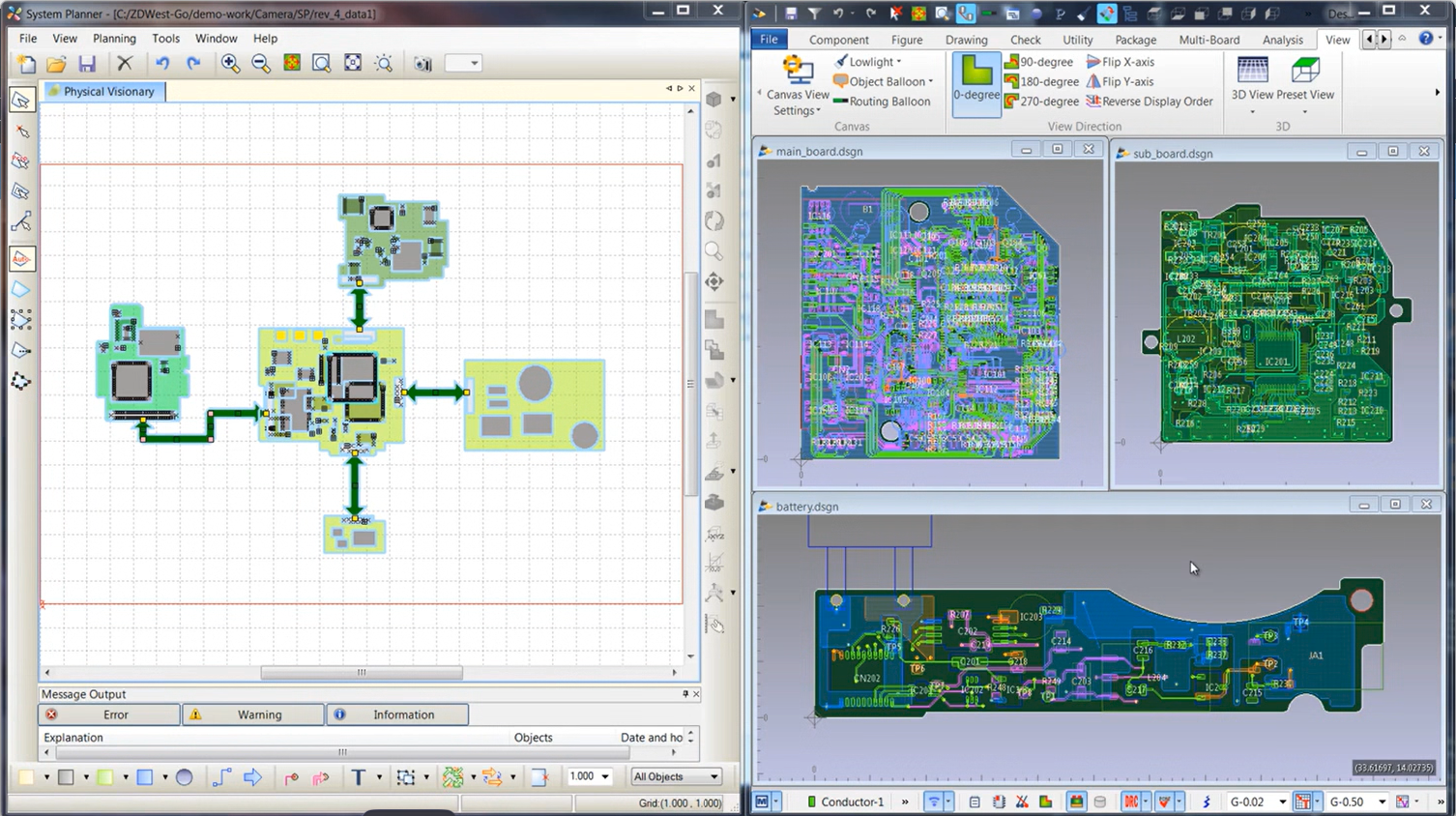
Within CR-8000, the functional and multi-board PCB design developed in System Planner can move into Design Gateway for schematic design and Design Force for PCB design.
Design Gateway supports logical circuit design and verification for single- and multi-board systems. It can also manage board-to-board signal continuity at the system level.
Design Force provides the physical design environment for individual boards and complete multi-board systems
PCB designers still make the detailed engineering decisions required for their boards. They define circuitry, select components, apply constraints, place parts, route connections, and perform board-level checks.
The difference is that they begin with a clearer understanding of each PCB’s role within the electronic subsystem.
This continuity also supports change management. When an architectural decision affects several boards, engineers can evaluate its broader impact rather than treating each PCB as an isolated update.
The objective is to preserve useful engineering context across design stages that would otherwise require separate coordination and manual data management.
A More Connected Approach to PCB Development
Modern PCB design still depends on board-level engineering excellence. Engineers must create accurate schematics, apply constraints, route complex connections, verify electrical behavior, and prepare reliable manufacturing data.
System-level PCB design does not replace these activities. It helps teams perform them within the right context.
By connecting architecture definition, multi-board planning, mechanical evaluation, and early verification, teams can make important decisions sooner and better understand the effects of those decisions.
CR-8000 supports this approach by connecting early electronic architecture with detailed schematic and PCB implementation through System Planner, Design Gateway, and Design Force.
For teams developing complex multi-board products, moving beyond single-board thinking is not simply a change in tools. It is a more coordinated approach to electronic design, from initial architecture through detailed implementation.
—
Explore CR-8000 to learn how Zuken supports system-level PCB design, multi-board planning, and connected PCB development.

-
Manager of Engineering Operations, SOZO Center at Zuken USA Inc.

- Blog

- Blog
- Blog
- Blog
Related Products and Resources
- Press Release
- Products

- Products
Building a competitive product today is much more difficult than a few years ago. Existing PCB-centric design processes are limited to a single PCB and do not provide the necessary tools for today’s competitive product development environment. PCB-centric design processes are falling behind.