
Tech Tip: Precise PCB Keepout Area Control with CR-8000
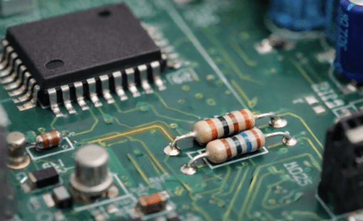
Modern PCB layouts demand precise routing control. As board designs become denser and constraints become more difficult to manage, PCB engineers need more flexibility than all-or-nothing keepout rules.
The Track Keepout feature in CR-8000 Design Force enables PCB designers to selectively allow traces or copper fills within designated keepout areas. This gives layout engineers more granular control over routing behavior while helping reduce DRC issues, routing inefficiencies, and unwanted electrical connections.
Why PCB Designers Use Keepout Areas
Keepout areas are protected regions on a PCB that restrict where conductive elements can be placed. PCB designers use them to prevent traces or copper fills from causing electrical, manufacturing, or reliability issues.
A PCB designer may define certain keepout zones to:
- Prevent traces from routing beneath high-speed devices where additional signals could introduce electrical noise or interference.
- Maintain required spacing around high-voltage circuitry to meet safety and clearance requirements.
- Block routing and copper placement near component bodies to avoid assembly or soldering problems.
As PCB layouts become denser and more complex, keepout areas help designers maintain control over routing and copper distribution throughout the board.
Why PCB Designers Need More Granular Keepout Control
Traditional keepout rules are often defined as all-or-nothing restrictions, blocking both routing and copper placement within a region. However, many PCB layouts require more selective control so designers can restrict one type of conductive element while still allowing another.
- Allow traces and vias, prevent copper fills: A designer may need traces and vias to pass through a constrained region near a component, while blocking copper fills that could create unintended electrical connections or spacing violations.
- Allow copper fills, prevent traces: A designer may want a ground copper fill beneath a sensitive device for shielding or thermal performance, while preventing traces from routing through the same area to reduce electrical noise or interference.
Without this level of control, engineers may create overly restrictive rules that complicate routing. In other cases, designers may override DRC warnings to achieve the desired layout, increasing the risk of costly errors and rework later in the design process.
How to Use the Track Keepout Feature in CR-8000 Design Force
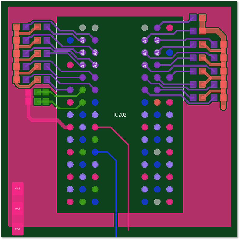
The Track Keepout feature works by combining designated keepout layers with configurable keepout rules. In CR-8000 Design Force, PCB designers define the keepout area and specify whether lines or area fills are allowed within that region.
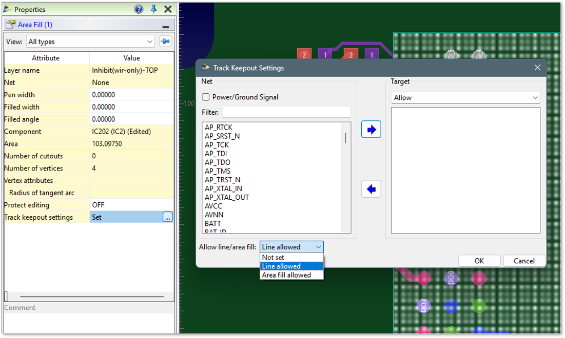
The feature uses these three steps:
- Create an “Inhibit track only” layer
- Define the keepout area geometry
- Set whether lines or area fills are allowed
With proper setup, traces and fills are automatically restricted in appropriate keepout zones.
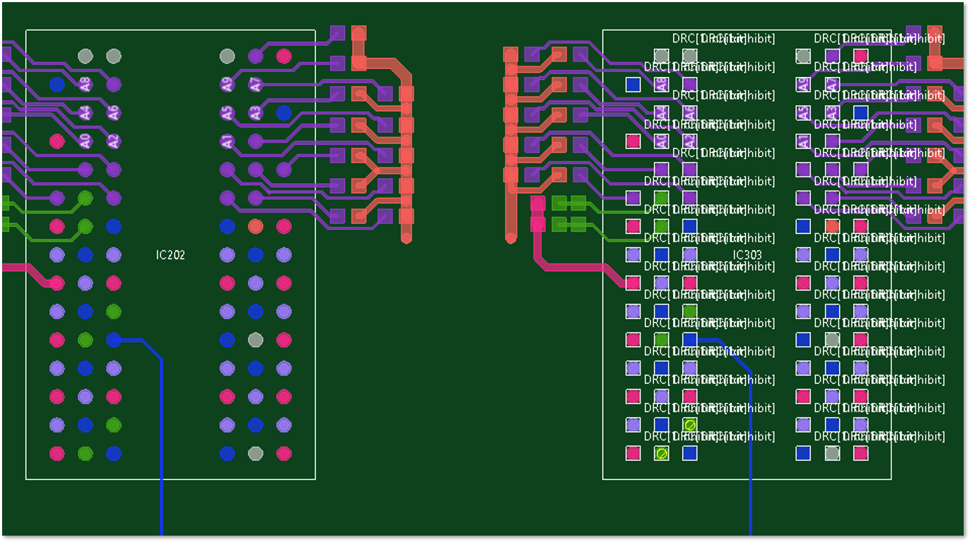
Bonus tip: Keepout areas are often associated with components. If the keepout is input on the board but not the component, the component pins trigger DRC errors. To reduce false DRC warnings, define the keepout area within the component footprint or use the “Make Figure into Component” feature in Design Force so the DRC engine correctly interprets the designer’s intent.
Who Benefits from the Track Keepout feature?
-
PCB Layout Engineers
Improve routing flexibility while maintaining precise control over copper placement and spacing restrictions. -
Signal Integrity Engineers
Reduce electrical noise and interference by controlling where traces and copper fills are permitted. -
Library and CAD Engineers
Create more accurate component footprint definitions and reduce false DRC warnings during layout.
See How Track Keepout Control Works
Next Steps: Strengthen Your PCB Design with CR-8000
Beyond Track Keepout control, CR-8000 Design Force provides advanced PCB layout and routing capabilities that help engineering teams manage increasingly dense and complex board designs. From configurable design rules to integrated DRC management, CR-8000 helps PCB designers improve routing efficiency while reducing layout errors and rework throughout the development process.
To learn more:
- Explore the CR-8000 product page
- Read another Tech Tip about maintaining signal integrity
- Watch this AI Place-and-Route webinar

-
Applications Engineer

- Blog

- Blog
- Blog

- Blog
Related Products and Resources
- Blog

- Webinar
- Products
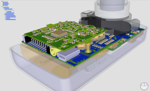
Design Force combines traditional 2D design with native 3D design and the latest human interface techniques, accelerated graphics and almost instantaneous rendering and refreshing. It is the fastest, most effective PCB design solution available today. Design Force enables design teams to layout their designs in the context of a complete system or product.

- Products
Building a competitive product today is much more difficult than a few years ago. Existing PCB-centric design processes are limited to a single PCB and do not provide the necessary tools for today’s competitive product development environment. PCB-centric design processes are falling behind.